

|
|
Double Segment Polarity Mark |
Post Reply 
|
| Author | |
RLS2004 
Advanced User 
Joined: 26 Jan 2012 Location: Seattle,WA Status: Offline Points: 51 |
 Post Options Post Options
") Thanks(0) Thanks(0)
 Quote Reply Quote Reply
 Topic: Double Segment Polarity Mark Topic: Double Segment Polarity MarkPosted: 29 May 2012 at 5:48pm |
|
If there is room, add a short ss segment to improve visibility of the pin 1 polarity.
|
|
 |
|
|
|
|
Tom H
Admin Group 

Joined: 05 Jan 2012 Location: San Diego, CA Status: Offline Points: 5716 |
Post Options
Thanks(0)
Quote Reply
Posted: 22 Oct 2012 at 9:59am |
|
We have decided that on many component families there is no room for double silkscreen outlines for Polarity Marking.
Instead, the new standard is the "Lack of Silkscreen" is the new polarity marker. Can you look at this QFN picture with the physical component installed and tell me where Pin 1 is? 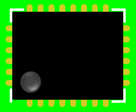 Nice solution for bottom only terminal parts and micro-miniature packages. |
|
|
|
|
Post Reply
|
|
| Tweet |
| Forum Jump | Forum Permissions You cannot post new topics in this forum You cannot reply to topics in this forum You cannot delete your posts in this forum You cannot edit your posts in this forum You cannot create polls in this forum You cannot vote in polls in this forum |


 Topic Options