

|
|
BGA PAD Mask Definition |
Post Reply 
|
| Author | |
mnperry 
Active User 
Joined: 12 Jan 2021 Status: Offline Points: 12 |
 Post Options Post Options
") Thanks(0) Thanks(0)
 Quote Reply Quote Reply
 Topic: BGA PAD Mask Definition Topic: BGA PAD Mask DefinitionPosted: 17 May 2023 at 6:24am |
|
I get the idea of either a reduction or increase in defining the land pad based on whether I am defining a collapsing or non-collapsing ball / land pattern. This is a percentage.
How is the solder and paste mask (excess) defined? Is there a manual calculation I have to do in the case of an increase in pad size so the mask will partly cover the land pad? In the calculator the solder mask excess is 0.00 no matter whether a collapsiong or non-collapsing ball is being used. 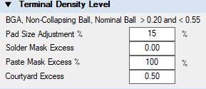 Also in the CAD translator, I see this. What is the UseMaskExpansionRules for? 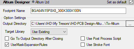 I suspect I am missing something obvious. Thanks.
|
|
 |
|
|
|
|
Tom H
Admin Group 

Joined: 05 Jan 2012 Location: San Diego, CA Status: Offline Points: 5718 |
Post Options
Thanks(0)
Quote Reply
Posted: 17 May 2023 at 8:37am |
|
Altium has its own Preference Rules and Solder Mask Swell is one of them.
UseMaskExpansionRules = no matter what solder mask is defined in Footprint Expert, use the Altium Preference settings. In other CAD tools (like PADS Layout), the solder mask defined in Footprint Expert is translated directly across. Everyone has there own solder mask swell. 0.05, 0.06, 0.07, 0.075, 0.08, 0.09, 0.10, etc. In a typical company PCB Library, every solder mask oversize is the same value. However, an example of changing times, Texas Instruments recommended solder mask swell on fine pitch and microminiature packages is 0.05 swell but in larger pin pitches and bigger packages the mfr. recommended solder mask swell is 0.07. For BGA's TI recommends rounded corner squares for solder mask. There are more and more semiconductors from TI that have complex solder mask shapes.  These semiconductors are becoming more mainstream every day.  |
|
|
|
|
Post Reply
|
|
| Tweet |
| Forum Jump | Forum Permissions You cannot post new topics in this forum You cannot reply to topics in this forum You cannot delete your posts in this forum You cannot edit your posts in this forum You cannot create polls in this forum You cannot vote in polls in this forum |


 Topic Options