|
|
IPC-J-STD-001 Gull Wing Leads and Solder Joints |
Post Reply 
|
| Author | |
Tom H 
Admin Group 

Joined: 05 Jan 2012 Location: San Diego, CA Status: Offline Points: 6074 |
 Post Options Post Options
") Thanks(0) Thanks(0)
 Quote Reply Quote Reply
 Topic: IPC-J-STD-001 Gull Wing Leads and Solder Joints Topic: IPC-J-STD-001 Gull Wing Leads and Solder JointsPosted: 26 Dec 2019 at 11:08am |
|
The Gull Wing lead is the second most popular terminal lead form on most PCB’s.
There are two things that are important here:
IPC-J-STD-001 does not put any emphasis on the Toe solder joint goal. It’s as though it’s insignificant. The Gull Wing Terminal Lead can extend to the end of the pad and even slightly beyond the pad and still pass J-STD-001 acceptance criteria.
However, IPC-J-STD-001 does have several comments on the
Gull Wing Terminal Heel solder joint. The F dimension.
Here is an image from a Vishay recommended land pattern. The Terminal Lead Tip to Tip dimension = 6.20 mm and the recommended land pattern dimension for the outside pads = 6.248 mm. This meets the IPC-J-STD-001 solder joint criteria, but not the IPC-7351 solder joint goal criteria. http://www.vishay.com/docs/68969/si4925dd.pdf
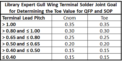
Here are the IPC-7351B Solder Joint Goal tables 3-2 &
3-3 for the Gull Wing Terminal Lead. Notice that the Toe and Heel solder joint
goals are the same value for every Gull Wing lead. Also notice that the difference
between Most, Nominal and Least Density Levels are in 0.20 mm increments. PCB
Libraries, Inc. believes that this margin between density levels is too steep.
The Most density level is too large and has too much solder and the least
density level is too small and does not have enough solder.
Gull Wing affects the component families SOP, QFP, SOT, SOD
and DPAK.
This is where PCB Libraries and IPC go our own separate way.
IPC-7351B Nominal Density Level recommends a 0.35 mm Toe and Heel regardless of
the component family, lead pitch and Terminal Lead Frame Thickness. The Lead-Frame
Thickness on a common DPAK is 0.65 mm but the Lead Thickness on a 0.50 mm pitch
QFP or SOP is 0.15 mm. They do not require the same Toe value
PCB Libraries, Inc. believes that the Toe value should equal
the Lead-Frame Thickness to show visible wetting in the Toe solder joint. Here
is a simple image of this philosophy.
PCB Libraries created an Incremental pad stack concept for Gull Wing Leads based on Terminal Lead Thickness, which is primarily based on the Terminal Pin Pitch.
PCB Libraries, Inc. believes that this margin between
density levels should be more subtle and swing 0.10 mm from the Nominal density
level to the Most and Least density level. If you compare IPC-7351 with the
original IPC-SM-782 land pattern standard that existed for 18 years, the SM-782
standard was about 0.10 mm larger than the 7351 Nominal.
PCB Libraries, Inc. in conjunction with our top tier customers, created an Incremental pad stack table based on the Terminal Lead Frame Thickness which is derived from the pin pitch.
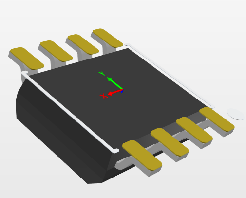
Download the Library Expert Excel spreadsheet Solder Joint Goal tables here – www.pcblibraries.com/downloads Also, if you are a Library Expert user, the Solder Joint Goal table Excel spreadsheet is already on your computer in this folder: C:\Program Files (x86)\PCB Libraries\Library Expert 2019\Documents\Library Expert Solder Joint Goal Tables.xlsx Here is an image of a real Gull Wing package with an adequate Toe Solder Joint. Not too big and not too small.
|
|
 |
|

|
|
|
|
|
Tom H
Admin Group
Joined: 05 Jan 2012 Location: San Diego, CA Status: Offline Points: 6074 |
Post Options
Thanks(0)
Quote Reply
Posted: 13 Jan 2020 at 5:52pm |
|
There is an exception to this rule and that is the DPAK gull wing lead thickness can be 0.65 mm and the Toe should be 0.50 mm for the best Toe Fillet.
The DPAK is a separate component family Terminal Lead Form in Library Expert with different Toe values than SOP, QFP, SOT and SOD. |
|
|
|
|
david.vrtaric
New User 
Joined: 27 Sep 2016 Status: Offline Points: 5 |
Post Options
Thanks(0)
Quote Reply
Posted: 27 Jul 2020 at 4:45am |
|
Hi Tom,
One question. I see the recommended Toe, Heel & Side solder joint goals from your tables (IPC-7351C Proposed Solder Joint Goal Tables for Least Density, but can you tell on what size do you apply these values from component datasheet? I apply these values to E dimension mean values from 2.40 mm and 1.80 mm or to max value 2.40 mm and also what L value do i use 0.46 or the mean of 0.46 and 0.26? Br.
|
|
|
|
|
Tom H
Admin Group
Joined: 05 Jan 2012 Location: San Diego, CA Status: Offline Points: 6074 |
Post Options
Thanks(0)
Quote Reply
Posted: 27 Jul 2020 at 8:32am |
|
No, this assumption is entirely incorrect.
The Solder Joint Goals are in addition to the Manufacturing Tolerances and the Component Package and Terminal Lead Min./Max. Tolerances. We use the IPC-7351 mathematical model that is illustrated in IPC-7351B. See the Surface Mount References Calculator for the math formula. It's in this folder on your computer: C:\Program Files (x86)\PCB Libraries\Library Expert 2019\Documents File Name: PCB_Library_Expert_SMD_Reference_Calculator |
|
|
|
|
david.vrtaric
New User
Joined: 27 Sep 2016 Status: Offline Points: 5 |
Post Options
Thanks(0)
Quote Reply
Posted: 27 Jul 2020 at 9:04am |
|
Hi Tom,
thanks for the fast replay. But how i can apply this calculator to SC70 package from the link? Because i'm also looking at document what is new in ipc-7351c page 38 an fog gull wing pad length is nominal L + toe + heel ? so for SC70 and nominal density = 0.35mm + 0.15mm + 0.2mm ? Br.
|
|
|
|
|
Tom H
Admin Group
Joined: 05 Jan 2012 Location: San Diego, CA Status: Offline Points: 6074 |
Post Options
Thanks(0)
Quote Reply
Posted: 27 Jul 2020 at 9:12am |
|
Use the SOT-23 Calculator for all Gull Wing leaded parts that have 3, 4, 5, 6 and 8 pins with various pin pitches.
IPC-7351C is not released and it's not going to contain all the new features that we wanted. Whatever version of IPC-7351C you have is not correct (unless you're on the 1-13 Land Pattern Committee and got a Working Draft from IPC). You cannot manually do the math to calculate an accurate pad stack and its location. You need a calculator. |
|
|
|
|
david.vrtaric
New User
Joined: 27 Sep 2016 Status: Offline Points: 5 |
Post Options
Thanks(0)
Quote Reply
Posted: 27 Jul 2020 at 9:19am |
|
i was looking at this document at page 38 https://dokumen.tips/documents/what-is-new-in-ipc-7351c-is-new-in-ipc-7351c-pcb-library-expert-fpx-library-multiple.html
 |
|
|
|
|
Tom H
Admin Group
Joined: 05 Jan 2012 Location: San Diego, CA Status: Offline Points: 6074 |
Post Options
Thanks(0)
Quote Reply
Posted: 27 Jul 2020 at 9:53am |
|
IPC did not accept the Proportional Pad Stack concept.
It was recommended but never accepted or approved. Everything (and I mean everything) in that Power Point presentation has been rejected by IPC. But PCB Libraries, Inc. implemented most of it in Library Expert (except the Proportional Pad Stack was thrown out because it was strictly based on Nominal Component Package Dimensions). However, the FED in Germany did pick up the Proportional Pad Stack model and published a book on it by Rainer Taube. |
|
|
|
|
Post Reply
|
|
| Tweet |
| Forum Jump | Forum Permissions You cannot post new topics in this forum You cannot reply to topics in this forum You cannot delete your posts in this forum You cannot edit your posts in this forum You cannot create polls in this forum You cannot vote in polls in this forum |


 Topic Options