
 |

|
Footprint Libraries |
Post Reply 
|
Page 12> |
| Author | |
ketan 
New User 
Joined: 29 Sep 2012 Location: india Status: Offline Points: 3 |
 Post Options Post Options
 Thanks(0) Thanks(0)
 Quote Quote  Reply Reply
 Topic: Footprint Libraries Topic: Footprint LibrariesPosted: 29 Sep 2012 at 9:16am |
|
Hi,
I need footprints for all the general componants like through-hole resistors for 1/4W, 1/2W, 1W and 5W and capacitors 10UF, 100UF, 1000UF Radial Lead and DIP package IC's and general commonly used audio amplifier IC's like TDA 2030. Can someone please share these footprints? It will be very much helpful to me and many other people I feel. Thanking all of you in advance. |
|
 |
|

|
|
 |
|
Tom H 
Admin Group 

Joined: 05 Jan 2012 Location: San Diego, CA Status: Offline Points: 6061 |
 Post Options Post Options
 Thanks(0) Thanks(0)
 Quote Quote  Reply Reply
 Posted: 29 Sep 2012 at 9:28am Posted: 29 Sep 2012 at 9:28am |
|
I take for granted that you use OrCAD Layout.
We can help provide you 10's of thousands of library parts for OrCAD Layout using the PCB Footprint Expert. Download it here for free - www.pcblibraries.com Install it and start building OrCAD Layout library parts. |
|
 |
|
budnoel 
Active User 

Joined: 16 Mar 2012 Status: Offline Points: 17 |
 Post Options Post Options
 Thanks(0) Thanks(0)
 Quote Quote  Reply Reply
 Posted: 21 Mar 2013 at 6:53am Posted: 21 Mar 2013 at 6:53am |
|
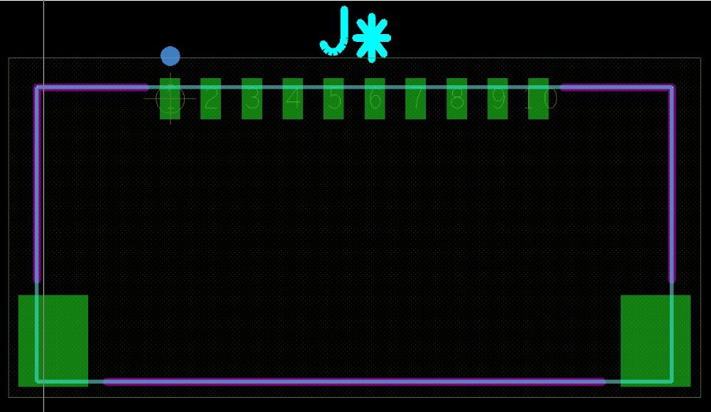
Hello - What is the recommended symbol origin for connectors? I've been using pin 1 for both SMT and PTH. Our engineers would prefer body center for the SMT but some of our connectors are difficult to determine where the body center is located. I've included an example.
 |
|
 |
|
Tom H 
Admin Group 

Joined: 05 Jan 2012 Location: San Diego, CA Status: Offline Points: 6061 |
 Post Options Post Options
 Thanks(0) Thanks(0)
 Quote Quote  Reply Reply
 Posted: 21 Mar 2013 at 7:32am Posted: 21 Mar 2013 at 7:32am |
|
Pin 1 is the most common 1st.
In the middle of a single row is 2nd. In the component body center is 3rd. The new "Package Designer" coming out this weekend in V2013 allows you to create the above footprint in a snap and you can relocate the origin anywhere you like. |
|
 |
|
ketan 
New User 
Joined: 29 Sep 2012 Location: india Status: Offline Points: 3 |
 Post Options Post Options
 Thanks(0) Thanks(0)
 Quote Quote  Reply Reply
 Posted: 21 Mar 2013 at 8:18am Posted: 21 Mar 2013 at 8:18am |
|
Thanks Tom,
Thanks again! |
|
 |
|
jameshead 
Expert User 
Joined: 20 Mar 2012 Location: Oxfordshire, UK Status: Offline Points: 576 |
 Post Options Post Options
 Thanks(1) Thanks(1)
 Quote Quote  Reply Reply
 Posted: 21 Mar 2013 at 9:06am Posted: 21 Mar 2013 at 9:06am |
|
If it's a surface-mount connector then I'll always put the footprint origin in the centre-of-body.
If it's a through-hole connector then I look at the connector type and what it's going to be connected to. If it's going to be a board-to-board connector then usually I will go for the centre-of-body since it makes things more straight forward when positioning opposing connectors on different boards. If it's a screw terminal or wire-to-board connector then I will go for pin 1. I find it useful sometimes when I put the origin on pin 1 to also put a marker on the "placement layer" (or what a PADS user would call layer 20) for the centre-of-body of the component as well - but make it visibly different from the normal component origin marker - to give me something to pick up on "snap" and place at a specific position. Since I work on a metric grid it helps with components with connections on a 2.54mm pitch, on those "grey-area" components that may end up being board-to-board in some cases. |
|
 |
|
Tom H 
Admin Group 

Joined: 05 Jan 2012 Location: San Diego, CA Status: Offline Points: 6061 |
 Post Options Post Options
 Thanks(0) Thanks(0)
 Quote Quote  Reply Reply
 Posted: 21 Mar 2013 at 12:27pm Posted: 21 Mar 2013 at 12:27pm |
|
Our PCB Footprint Expert "Lite" has an interface to OrCAD Layout.
Check it out and let us know how it works for you. We take suggestions for improvements even from those who never purchase from us. Here are the import instructions - |
|
 |
|
sundar 
New User 
Joined: 09 Sep 2013 Status: Offline Points: 14 |
 Post Options Post Options
 Thanks(0) Thanks(0)
 Quote Quote  Reply Reply
 Posted: 09 Sep 2013 at 10:10pm Posted: 09 Sep 2013 at 10:10pm |
|
I need footprint for QFN 56 pin 8X8mm 0.5 pitch
|
|
 |
|
Nick B 
Admin Group 

Joined: 02 Jan 2012 Status: Offline Points: 1994 |
 Post Options Post Options
 Thanks(0) Thanks(0)
 Quote Quote  Reply Reply
 Posted: 10 Sep 2013 at 1:21pm Posted: 10 Sep 2013 at 1:21pm |
|
Have you tried the Library Expert Lite? It's available from our main webpage, or via the Download link at the top (banner).
Nick |
|
 |
|
saravananjsrs 
New User 
Joined: 17 Dec 2013 Location: tamilnadu Status: Offline Points: 1 |
 Post Options Post Options
 Thanks(0) Thanks(0)
 Quote Quote  Reply Reply
 Posted: 19 Dec 2013 at 8:17am Posted: 19 Dec 2013 at 8:17am |
|
please sent all tda ic st microelectronics foot prints including tda7483,tda7560 and KIA6210
|
|
 |
|
Post Reply 
|
Page 12> |
| Tweet |
| Forum Jump | Forum Permissions  You cannot post new topics in this forum You cannot reply to topics in this forum You cannot delete your posts in this forum You cannot edit your posts in this forum You cannot create polls in this forum You cannot vote in polls in this forum |