
 |

|
Confused about pad size |
Post Reply 
|
| Author | |
magnus.lictor 
Advanced User 
Joined: 27 Aug 2012 Location: Amsterdam, NL Status: Offline Points: 64 |
 Post Options Post Options
 Thanks(0) Thanks(0)
 Quote Quote  Reply Reply
 Topic: Confused about pad size Topic: Confused about pad sizePosted: 20 Mar 2023 at 6:57am |
|
LS,
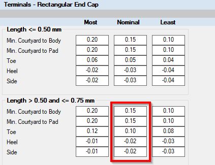
I am creating a footprint for an 0201 resistor and I am a bit confused about the pads for the generated component. The size of the 0201 is defined as 0.60mmx0.30mm, with a 0.03 tolerance. The terminal width = 0.15x0.30mm.  The visible grid is 0.01mm. The settings in the Footprint Expert fort the pad size are;  The placement tolerance is set to the default 0.025mm The generated part however has a toe value of 0.148mm. I do not understand how this value is calculated. The same applies for the side and heel value. I would expect it to fall inside the terminal. What am I missing ? Regards, Charles |
|
 |
|

|
|
 |
|
Tom H 
Admin Group 

Joined: 05 Jan 2012 Location: San Diego, CA Status: Offline Points: 6029 |
 Post Options Post Options
 Thanks(1) Thanks(1)
 Quote Quote  Reply Reply
 Posted: 20 Mar 2023 at 8:35am Posted: 20 Mar 2023 at 8:35am |
|
You are missing the package tolerances.
The package tolerances are included in the mathematical model to determine the pad size. Make all the package tolerances 0.00 and see what happens. The Fabrication and Assembly tolerances are also used in the mathematical model to determine the pad size. Turn them to 0.00 to see the results. You can also turn the negative values in the solder joint goals to 0.00 and see what happens. |
|
 |
|
Post Reply 
|
|
| Tweet |
| Forum Jump | Forum Permissions  You cannot post new topics in this forum You cannot reply to topics in this forum You cannot delete your posts in this forum You cannot edit your posts in this forum You cannot create polls in this forum You cannot vote in polls in this forum |