
 |

|
Dual Flat No-Lead (DFN 2-Pin) Non-Symmetrical |
Post Reply 
|
| Author | |
JDPrymak 
New User 
Joined: 04 Apr 2013 Location: SC Status: Offline Points: 13 |
 Post Options Post Options
 Thanks(1) Thanks(1)
 Quote Quote  Reply Reply
 Topic: Dual Flat No-Lead (DFN 2-Pin) Non-Symmetrical Topic: Dual Flat No-Lead (DFN 2-Pin) Non-SymmetricalPosted: 05 Apr 2013 at 5:58am |
|
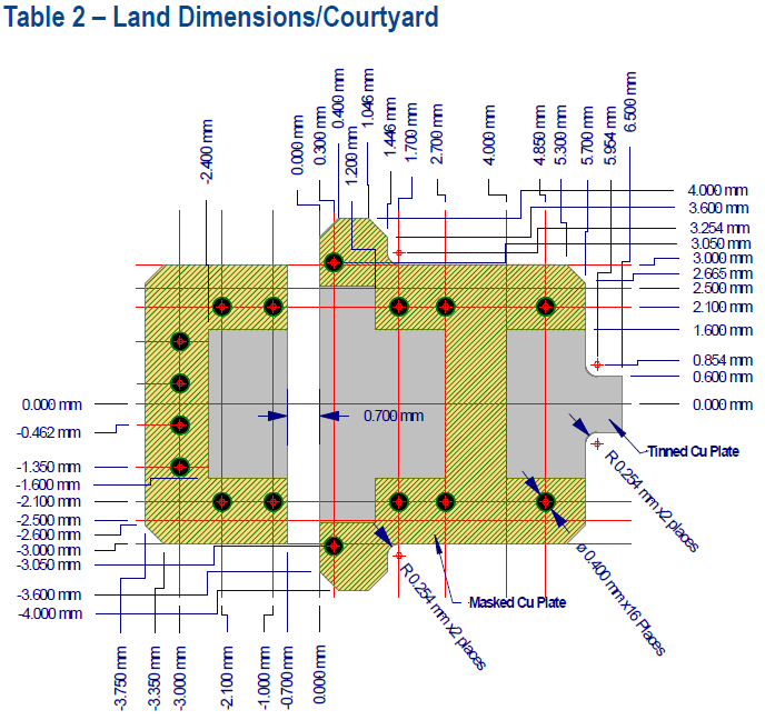
We need the land patterns to be non-symmetrical for a polar capacitor. Cathode plate is larger to allow greater heat dissipation, and polar mounting.
|
|
 |
|

|
|
 |
|
Tom H 
Admin Group 

Joined: 05 Jan 2012 Location: San Diego, CA Status: Offline Points: 5993 |
 Post Options Post Options
 Thanks(0) Thanks(0)
 Quote Quote  Reply Reply
 Posted: 05 Apr 2013 at 6:52am Posted: 05 Apr 2013 at 6:52am |
|
Could you please attach a web-link to the datasheets?
Our programmers need to see what your request is. They don't want to assume anything. Aside that, the new "Package Designer" will be released this weekend in V2013 and you can create many non-standard library parts. You can even import ASCII files with X,Y coordinates and pin names for padstack placement. |
|
 |
|
JDPrymak 
New User 
Joined: 04 Apr 2013 Location: SC Status: Offline Points: 13 |
 Post Options Post Options
 Thanks(1) Thanks(1)
 Quote Quote  Reply Reply
 Posted: 05 Apr 2013 at 8:12am Posted: 05 Apr 2013 at 8:12am |
|
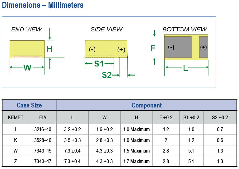
Here's a link to the T528 Low ESL. Facedown Tantalum Polymer Capacitors. The terminal dimensions are on page 4. The pad dimensions on page 7 are for the W and Z case, to allow a low ESL connection to the PCB and to allow connection to competitor's three-terminal device. The competitor created a three-terminal device, but there are two cathode connections. The cathode connection is broken into two to eliminate huge disparities in solder pod areas that could cause the larger cathode plate to lift chip and break anode pad connection. On our 7343 device we have only two terminals, anode and larger cathode, but recommend using two solder pads for the cathode to eliminate the propensity to lift. We do not believe that three solder pads are necessary for the smaller case devices.
|
|
 |
|
Tom H 
Admin Group 

Joined: 05 Jan 2012 Location: San Diego, CA Status: Offline Points: 5993 |
 Post Options Post Options
 Thanks(0) Thanks(0)
 Quote Quote  Reply Reply
 Posted: 05 Apr 2013 at 12:49pm Posted: 05 Apr 2013 at 12:49pm |
|
You're correct that if you just want to use the Kemet Capacitor you do not need 3 pads.
 And this land pattern is "over the top" detailed.  You can create a good Footprint using the "Molded Body" component family and then select the "Footprint" tab to enter the mfr. pad sizes and spacing. I think the center pad "wings" are for the alternate part. |
|
 |
|
Humberto222 
New User 
Joined: 05 Apr 2013 Status: Offline Points: 1 |
 Post Options Post Options
 Thanks(0) Thanks(0)
 Quote Quote  Reply Reply
 Posted: 18 Jul 2013 at 7:48am Posted: 18 Jul 2013 at 7:48am |
|
Did you mean Component tab ? .... to fill in there the lead dimensions
|
|
 |
|
Tom H 
Admin Group 

Joined: 05 Jan 2012 Location: San Diego, CA Status: Offline Points: 5993 |
 Post Options Post Options
 Thanks(0) Thanks(0)
 Quote Quote  Reply Reply
 Posted: 18 Jul 2013 at 12:02pm Posted: 18 Jul 2013 at 12:02pm |
|
You fill in the component dimensions in the "Component Tab"
You fill in the mfr. recommended pattern in the "Footprint Tab" |
|
 |
|
Post Reply 
|
|
| Tweet |
| Forum Jump | Forum Permissions  You cannot post new topics in this forum You cannot reply to topics in this forum You cannot delete your posts in this forum You cannot edit your posts in this forum You cannot create polls in this forum You cannot vote in polls in this forum |