

|
|
Lead Width on Axial Through Hole |
Post Reply 
|
| Author | |
jameshead 
Expert User 

Joined: 20 Mar 2012 Location: Oxfordshire, UK Status: Offline Points: 576 |
 Post Options Post Options
") Thanks(0) Thanks(0)
 Quote Reply Quote Reply
 Topic: Lead Width on Axial Through Hole Topic: Lead Width on Axial Through HolePosted: 07 Mar 2013 at 2:40am |
|
The PDF for IPC-7251 states:
W = Maximum Lead Width (or Component Lead Diameter) In Through Hole > Axial though users have to enter both Min and Max values for b and the calculated footprint name uses the nominal value for b, for W, and not Maximum Lead Width as I expected. IPC-2222 says "no greater than 0.7 mm (level A) over minimum lead diameter" so I guess that's why FPX has a mandatory field for a Min value for b in Axial (?) but if I'm creating a footprint in a program like FPX I am more concerned with the maximum lead diameter and the "No less than 0.25 mm over maxium lead diameter". |
|
 |
|

|
|
|
|
|
Jeff.M
Admin Group 

Joined: 16 May 2012 Location: San Diego Status: Offline Points: 501 |
Post Options
Thanks(0)
Quote Reply
Posted: 07 Mar 2013 at 9:11am |
|
A maximum value is required to calculate the hole.
A minimum value is required to get the nominal value which is used in the footprint name.
|
|
|
|
|
jameshead
Expert User
Joined: 20 Mar 2012 Location: Oxfordshire, UK Status: Offline Points: 576 |
Post Options
Thanks(0)
Quote Reply
Posted: 07 Mar 2013 at 9:14am |
|
Hi Jeff, thanks for the reply.
My observation is that the PDF guide for IPC-7251 says: W = Maximum Lead Width (or Component Lead Diameter) So, W should be taking the maximum and not the nominal dimension. |
|
|
|
|
jameshead
Expert User
Joined: 20 Mar 2012 Location: Oxfordshire, UK Status: Offline Points: 576 |
Post Options
Thanks(0)
Quote Reply
Posted: 11 Mar 2013 at 7:33am |
|
This behavour in FPX hasn't changed in the v47 Beta today.
The PDF guide for IPC-7251 naming says: Diodes, Axial Diameter Horizontal Mounting .......................................DIOAD + Lead Spacing + W Lead Width + L Body Length + D Body Diameter And on page 3: W = Maximum Lead Width (or Component Lead Diameter) The way I read this was that W is always the Maximum whether it's the lead width or component lead diameter, but Jeff's saying W is nominal. |
|
|
|
|
Tom H
Admin Group

Joined: 05 Jan 2012 Location: San Diego, CA Status: Offline Points: 6075 |
Post Options
Thanks(0)
Quote Reply
Posted: 15 Mar 2013 at 8:24pm |
|
The Calculator requires Maximum to determine the hole size per IPC-7251 (which is currently on the table by IPC for review for release (finally)).
The component dimensions require the Minimum so the Calculator can determine the value for the Footprint name. Every value in the Footprint Name is a "Nominal" component package dimension with one exception - "Height" |
|
|
|
|
Naveed Khan
Active User 
Joined: 12 Mar 2013 Location: India Status: Offline Points: 20 |
Post Options
Thanks(0)
Quote Reply
Posted: 18 Mar 2013 at 1:52am |
|
Hi Tom,
How to calculate pitch for axial lead components? IF mounted horizontally and vertically? |
|
|
|
|
Tom H
Admin Group
Joined: 05 Jan 2012 Location: San Diego, CA Status: Offline Points: 6075 |
Post Options
Thanks(0)
Quote Reply
Posted: 18 Mar 2013 at 6:27am |
|
The PCB Footprint Expert has a "Utilities" button in the Main Toolbar. Select the "Axial Leadform Calculator" option and this menu will appear -
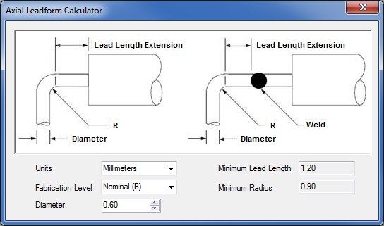 I hope this helps... |
|
|
|
|
jameshead
Expert User
Joined: 20 Mar 2012 Location: Oxfordshire, UK Status: Offline Points: 576 |
Post Options
Thanks(0)
Quote Reply
Posted: 20 Mar 2013 at 8:41am |
|
I understand but I think the PDF for the PCB Libraries Footprint Naming Convention for Standard TH Components on page 3 confuses users since it says:
W = Maximum Lead Width (or Component Lead Diameter) |
|
|
|
|
Tom H
Admin Group
Joined: 05 Jan 2012 Location: San Diego, CA Status: Offline Points: 6075 |
Post Options
Thanks(1)
Quote Reply
Posted: 20 Mar 2013 at 12:31pm |
|
I agree that we need to clarify Wmax for hole calculation and Wnom for Footprint Name.
|
|
|
|
|
Post Reply
|
|
| Tweet |
| Forum Jump | Forum Permissions You cannot post new topics in this forum You cannot reply to topics in this forum You cannot delete your posts in this forum You cannot edit your posts in this forum You cannot create polls in this forum You cannot vote in polls in this forum |


 Topic Options