

|
|
Some Default Settings missed - 2021.02 |
Post Reply 
|
| Author | |
Olaf.MuellerAE 
Active User 
Joined: 27 Feb 2015 Status: Offline Points: 28 |
 Post Options Post Options
") Thanks(0) Thanks(0)
 Quote Reply Quote Reply
 Topic: Some Default Settings missed - 2021.02 Topic: Some Default Settings missed - 2021.02Posted: 16 Apr 2021 at 1:48am |
|
Hello All,
i missed some default settings. - "Pad Size Roundoff" for the TH Terminals - "Solder Mask Annular Expansion" - "Paste Mask (% of Pad Size)" Also when the padstack is created it generates wrong pad names. I checked the demo values for Chip Resistor and set "Solder mask .." to 0.1 and the Paste to 90% the program generates a name like in the picture in 2 diffrent versions. 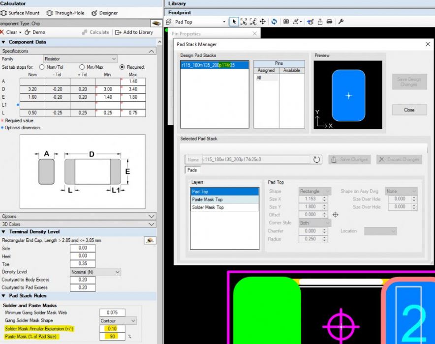 Best Regards Olaf Mueller
|
|
 |
|

|
|
|
|
|
Tom H
Admin Group 

Joined: 05 Jan 2012 Location: San Diego, CA Status: Offline Points: 6070 |
Post Options
Thanks(0)
Quote Reply
Posted: 16 Apr 2021 at 8:07am |
|
You have "File > Options > Pad Stack Rules > SMD Solder and Paste Masks" to globally set your Solder Mask and Paste Mask for all footprints.
The Round-off is new in V2021 Console Options - Decimal Place Accuracy goes from 2 - 6 places for minimum and maximum. The defaults are currently 2 minimum and 3 maximum but you can set it to whatever you what for low or high resolution. |
|
|
|
|
Post Reply
|
|
| Tweet |
| Forum Jump | Forum Permissions You cannot post new topics in this forum You cannot reply to topics in this forum You cannot delete your posts in this forum You cannot edit your posts in this forum You cannot create polls in this forum You cannot vote in polls in this forum |


 Topic Options