

|
|
Standard Chip Component Dimensions |
Post Reply 
|
Page 12> |
| Author | |
drj-bbe 
Advanced User 
Joined: 08 Jul 2015 Status: Offline Points: 71 |
 Post Options Post Options
") Thanks(1) Thanks(1)
 Quote Reply Quote Reply
 Topic: Standard Chip Component Dimensions Topic: Standard Chip Component DimensionsPosted: 08 Jul 2015 at 3:28am |
|
Hello,
I am trying to find a standard land pattern for chip resistor or capacitor, ex. 0402, 0603, etc. But one chip component may have different tolerance between each manufacturer, and land pattern calculated by Library Expert Pro will be different if according to component datasheet. If like this then I cannot get uniform land pattern design for one type component on board.
Is there a Industrial Standard for components package dimension? or some suggestions to make standard land pattern for one type component?
|
|
 |
|

|
|
|
|
|
Tom H
Admin Group 

Joined: 05 Jan 2012 Location: San Diego, CA Status: Offline Points: 6088 |
Post Options
Thanks(1)
Quote Reply
Posted: 08 Jul 2015 at 7:50am |
|
There are no EIA, JEDEC or IPC standards on chip size dimensions.
Here is the closest you will get to the Standard Case Sizes but good luck trying to find a manufacturer that uses these dimensions. Notice that the Height and Tolerances are missing because that is unique for every manufacturer. And the Height plays into the Toe solder joint calculation and the tolerances affect every aspect of the Land Pattern (footprint).  Download the document "Surface Mount Components" here - www.pcblibraries.com/downloads It illustrates all the various types of SMD packages and the variety of Chip components. |
|
|
|
|
drj-bbe
Advanced User
Joined: 08 Jul 2015 Status: Offline Points: 71 |
Post Options
Thanks(1)
Quote Reply
Posted: 08 Jul 2015 at 7:38pm |
|
Thanks for your reply.
Yes, Height and Tolerances can afftect land pattern size, and it is unique for every manufacturer.
But I cannot make unique land pattern for every manufacturer for an ex. 0603 component. I peffer to use only one land pattern for all brand 0603 components, not make many land patterns for a standard chip part in our library.
Could you please give your advice on this?
|
|
|
|
|
Tom H
Admin Group
Joined: 05 Jan 2012 Location: San Diego, CA Status: Offline Points: 6088 |
Post Options
Thanks(1)
Quote Reply
Posted: 09 Jul 2015 at 9:03am |
|
Let's figure out what you really want. Do you want to use the same footprint for every 0603 Chip component in the electronics industry regardless of their tolerance and package height?
 |
|
|
|
|
drj-bbe
Advanced User
Joined: 08 Jul 2015 Status: Offline Points: 71 |
Post Options
Thanks(1)
Quote Reply
Posted: 09 Jul 2015 at 6:14pm |
|
Sorry, I just want to use the same footprint for every 0603 Capacitor and Resistor regardless of their tolerance and package height.
|
|
|
|
|
Tom H
Admin Group
Joined: 05 Jan 2012 Location: San Diego, CA Status: Offline Points: 6088 |
Post Options
Thanks(1)
Quote Reply
Posted: 09 Jul 2015 at 8:09pm |
|
Here is the 2016 J-STD-001 SMD Proportional pad stack table for pad size calculations for Chip components. The Courtyard Excess has a 0.25 mm limiter on it, but all the percentages and values are user definable.
 Good luck with finding a single footprint to successfully accommodate every 0603 package. The Height is the main driver of this component lead form. Issue: if you use a 0603 land pattern considering the highest package, you may be dumping too much solder on an 0603 that is 50% of that height, introducing potential tomb-stoning. This new Proportional SMD technology will be available in the V2016 Library Expert. |
|
|
|
|
drj-bbe
Advanced User
Joined: 08 Jul 2015 Status: Offline Points: 71 |
Post Options
Thanks(1)
Quote Reply
Posted: 09 Jul 2015 at 8:40pm |
|
Many thanks for your feedback on this.
In order to understand fully the table you provided, I tried to find the table in IPC-J-STD-001F, but not see it. For 2016 J-STD-001, is it new version? I didn't find it in IPC website, only find F version.
|
|
|
|
|
Tom H
Admin Group
Joined: 05 Jan 2012 Location: San Diego, CA Status: Offline Points: 6088 |
Post Options
Thanks(1)
Quote Reply
Posted: 10 Jul 2015 at 8:56am |
|
This is new (unreleased) technology that we are testing this summer. It might be added to IPC-7351C but IPC wants it fully tested first.
I am a CIT trainer and teach hand soldering techniques to students. The J-STD-001 has guidelines for minimum and maximum solder joint goal ranges. Every Terminal Lead form has it's specific percentages for pad size calculations. Example: Gull Wing lead is based on percentage of the pin pitch. I'm just giving you a glimpse of the near future that you will not find in any publication today, will be in every standard next year. |
|
|
|
|
drj-bbe
Advanced User
Joined: 08 Jul 2015 Status: Offline Points: 71 |
Post Options
Thanks(1)
Quote Reply
Posted: 12 Jul 2015 at 7:03pm |
|
Thanks for your information.
There is a principles in IPC-7351B for 0603 component below. It seems different with the table you provided. The current principles will be replaced by new technology, right? 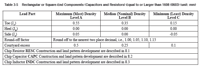 |
|
|
|
|
Tom H
Admin Group
Joined: 05 Jan 2012 Location: San Diego, CA Status: Offline Points: 6088 |
Post Options
Thanks(1)
Quote Reply
Posted: 12 Jul 2015 at 7:30pm |
|
That is the correct table for the 2010 version of IPC-7351B.
For your 0603, it falls in the large component type and the same solder joint rules apply in both the IPC-7351B and IPC-7351C. Here is the updated table for IPC-7351C and this is in V2015.15 of Library Expert Pro, Lite and Viewer for the smaller chip sizes. As you can see, 0402, 0201 and 01005 have different Toe goals to prevent tomb-stoning.  |
|
|
|
|
Post Reply
|
Page 12> |
| Tweet |
| Forum Jump | Forum Permissions You cannot post new topics in this forum You cannot reply to topics in this forum You cannot delete your posts in this forum You cannot edit your posts in this forum You cannot create polls in this forum You cannot vote in polls in this forum |


 Topic Options