

|
|
Suggestions how to generate a 4 terminal MLCC |
Post Reply 
|
| Author | |
Iain-Trakka 
Active User 
Joined: 19 Oct 2021 Status: Offline Points: 14 |
 Post Options Post Options
") Thanks(0) Thanks(0)
 Quote Reply Quote Reply
 Topic: Suggestions how to generate a 4 terminal MLCC Topic: Suggestions how to generate a 4 terminal MLCCPosted: 18 Dec 2023 at 5:01am |
|
Hello,
I'm curious to understand how one would generate a 4 terminal MLCC? Reference Part: EMCT101W103M1GV001E I do not see any 'good' starting component types... Any insight would be greatly appreciated, Thank you in advance, Iain
|
|
 |
|

|
|
|
|
|
Tom H
Admin Group 

Joined: 05 Jan 2012 Location: San Diego, CA Status: Offline Points: 6088 |
Post Options
Thanks(0)
Quote Reply
Posted: 18 Dec 2023 at 9:46am |
|
You need to use the mfr. recommended pattern and create the Footprint in FP Designer.
There is no information on solder joint goals for this non-standard Chip package with 3 pins. The mfr. needs to provide the pad stack information. |
|
|
|
|
Iain-Trakka
Active User
Joined: 19 Oct 2021 Status: Offline Points: 14 |
Post Options
Thanks(1)
Quote Reply
Posted: 06 Jan 2024 at 1:39pm |
|
Tom,
Thank you for your response and suggestion - I've reached out to the mfg. for their input... I'll post results here, if possible. Regards, Iain
|
|
|
|
|
Iain-Trakka
Active User
Joined: 19 Oct 2021 Status: Offline Points: 14 |
Post Options
Thanks(0)
Quote Reply
Posted: 12 Jan 2024 at 5:59pm |
|
Tom,
The mfg. came back with land pattern recommendations for the copper layer only, solder/paste mask were not provided. is this something that I could request your assistance with via POD request? (or request the part entirely...) Look forward to your comments, Iain
|
|
|
|
|
Tom H
Admin Group
Joined: 05 Jan 2012 Location: San Diego, CA Status: Offline Points: 6088 |
Post Options
Thanks(0)
Quote Reply
Posted: 12 Jan 2024 at 6:08pm |
|
Paste Mask is normally 1:1 scale of the pad size.
A PCB Library can have Solder Mask 2 ways:
|
|
|
|
|
Iain-Trakka
Active User
Joined: 19 Oct 2021 Status: Offline Points: 14 |
Post Options
Thanks(0)
Quote Reply
Posted: 13 Jan 2024 at 4:12am |
|
Tom,
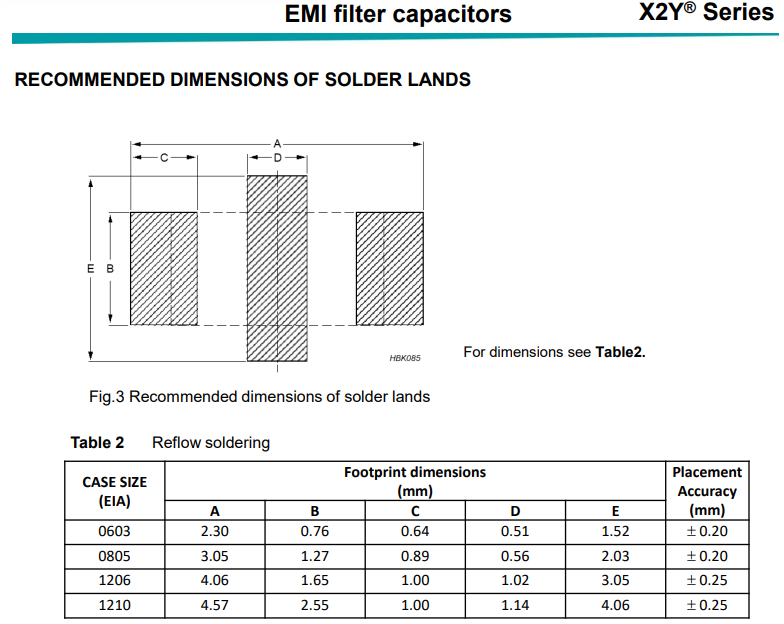
Thank you for responding - I believe I missed sharing some context on what was puzzling me... The part has 4-leads, yet the provided land pattern is three terminals (See Figure 3. Page 10, link below): Reference: https://productfinder.pulseelectronics.com/api/open/part-attachments/datasheet/CX0805MRX7R9BB153 (Note, yes this is a different part that I originally stated, yet FP is comparable and it is published data) Knowing that we'd end up connecting copper between the center two pins (as shown above), would we also extend the mask/paste completely across this center pin? Does it make sense to have exposed copper/paste directly under the center of the ceramic body? Other land patterns that I've seen, all had 4 distinct solder/paste areas (regardless of the copper shapes below)... Look forward to your comments. Regards, Iain
|
|
|
|
|
Tom H
Admin Group
Joined: 05 Jan 2012 Location: San Diego, CA Status: Offline Points: 6088 |
Post Options
Thanks(0)
Quote Reply
Posted: 13 Jan 2024 at 10:05am |
|
You have Pin 1 (left), Pin 2 (right) and Pin 3 (Center).
 |
|
|
|
|
Iain-Trakka
Active User
Joined: 19 Oct 2021 Status: Offline Points: 14 |
Post Options
Thanks(0)
Quote Reply
Posted: 13 Jan 2024 at 11:31am |
|
Tom,
Looking at figure 2, there are 4 distinct pins: 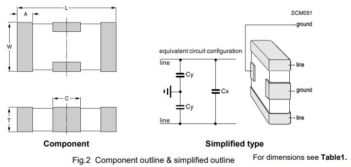 |
|
|
|
|
Tom H
Admin Group
Joined: 05 Jan 2012 Location: San Diego, CA Status: Offline Points: 6088 |
Post Options
Thanks(0)
Quote Reply
Posted: 13 Jan 2024 at 11:38am |
|
Makes no difference.
Use the mfr. recommended pattern. |
|
|
|
|
Iain-Trakka
Active User
Joined: 19 Oct 2021 Status: Offline Points: 14 |
Post Options
Thanks(0)
Quote Reply
Posted: 13 Jan 2024 at 12:11pm |
|
Okay Tom,
Thank you for the insight. Regards, Iain
|
|
|
|
|
Post Reply
|
|
| Tweet |
| Forum Jump | Forum Permissions You cannot post new topics in this forum You cannot reply to topics in this forum You cannot delete your posts in this forum You cannot edit your posts in this forum You cannot create polls in this forum You cannot vote in polls in this forum |


 Topic Options