3D STEP to VRML
Printed From: PCB Libraries Forum
Category: PCB Footprint Expert
Forum Name: Questions & Answers
Forum Description: issues and technical support
URL: https://www.PCBLibraries.com/forum/forum_posts.asp?TID=976
Printed Date: 20 Apr 2026 at 6:52pm
Topic: 3D STEP to VRML
Posted By: dwaltoneng
Subject: 3D STEP to VRML
Date Posted: 17 Jun 2013 at 2:27pm
|
Has anyone any suggestions on converting 3D STEP to VRML? Or for simplifying the VRML file? |
Replies:
Posted By: chrisa_pcb
Date Posted: 17 Jun 2013 at 5:29pm
|
Given that VRML is a markup language, the size is understandable. Right now we're focusing on getting all of the families(both surface mount and throughhole) to work and getting everything stable before even considering outputting to alternate formats. STEP 3D is the core as it seemed to provide the most compatibility across the board with the most number of programs, and actually ended up being fairly easy to work with once I understood and got the code setup for it. . And it sounds from your comments like DipTrace has problems when the VRML file gets fairly large(and the generated STEP 3D files can get fairly large, especially the ones with filleted corners and what not). |
Posted By: jameshead
Date Posted: 18 Jun 2013 at 1:02am
|
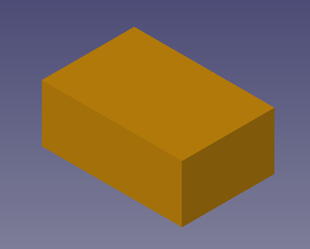
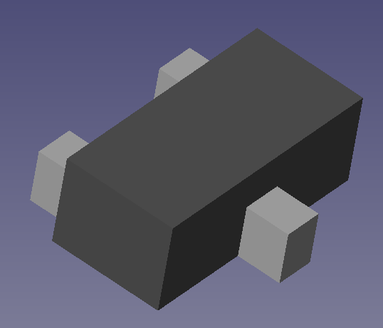
At the moment I either grab a 3D model from the manufacturers website or use FreeCAD to knock up something. I have been meaning to look at the STEP output from FPX but your comment "the generated STEP 3D files can get fairly large, especially the ones with filleted corners and what not" raises a red flag. Pulsonix works with both IDF and STEP files. It works with STEP files by importing a STEP file for a PCB that has been output from an MCAD program, or exporting a STEP file of board and components. Pulsonix will either use an existing STEP file for a component or create one based on the component type and if you've specified anything in the Pulsonix 3D viewer. If you have an existing STEP model you can place it in a folder, then in the footprint in the Pulsonix library (or the part) place three attributes to point to the STEP file filename, X/Y/Z rotation, and X/Y/Z offset. The biggest hassle when dealing with STEP files downloaded from manufacturers is the X/Y/Z rotations and offsets which appear to be random and vary between parts, including parts from the same manufacturers. To be honest we found the more elaberate manufacturer-supplied STEP files and Pulsonix generated STEP models for components to be a hassle for our MCAD Engineers when they imported into Solidworks since Pulsonix was creating a fancy component body with bended legs and terminals on chip components. They've told me that this is a hassle for them to deal with, increasing complexity and file size unnecessarily. They are only interested in a simple space model - they don't want or need fancy chamfers on IC bodies that take up file space in the STEP file and when processing the models in Solidworks. With that in mind I began using FreeCAD recently to create some simple STEP models. All we need for a chip component is a single cube of the maximum size, whilst all we need for something like a SOP chip is a cube for the body and a couple of cubes for the two rows of legs, and for SOT-23s, a cube for the body and a cube for each leg. See these examples: Chip CAP:  SOT-23  SOP or SOIC  I've not got around to asking for a demo of the sTEP from FPX yet but if you're putting the jazzy bits in then I'd probably not be interested in it. A choice might be useful between a simple block STEP file or a whistles-and-bells STEP file. |
Posted By: Tom H
Date Posted: 18 Jun 2013 at 7:07am
|
Yes, large Pin Count BGA STEP files can be 35MB but the average 3D STEP file is less than 100KB each. The 3D STEP files from the PCB Library Expert (LE) are High Quality and you create them with the same button you create Footprints. They have the same rotation, orign and name as the Footprint. And they're 100% customized for every Footprint. I think once you try the 3D STEP feature in LE you'll never use anything else. It's just too easy, especially with the "Parts on Demand" (POD) project that will have millions of component mfr. part numbers at your fingertips. |
Posted By: jameshead
Date Posted: 18 Jun 2013 at 7:40am
|
It's the "High Quality" label that might be an issue. It's not me that needs to be persueded when it comes to STEP models from FPX - it's the Mechanical CAD Engineers here using Solidworks. Here we have two of them (they're nice chaps really, even when they're making the PCB profiles smaller!). We use Solidworks and they are the ones that are saying that the elaborate STEP models with the modeled terminals are not suitable for what they want. They have to do extra work on them. I come from an Electronics background and have only just started to "play" with FreeCAD so I'm not totally familiar with how they are taking and using this data but the feedback they've been giving me is that the simple cube shapes are a lot easier and quicker for them to work with in Solidworks. |
Posted By: Tom H
Date Posted: 18 Jun 2013 at 7:51am
|
I use SolidWorks too. Did you download our 3D STEP for the Component Familes supported in the PCB Library Expert? http://www.pcblibraries.com/downloads/Guidelines!Component_Families.asp" rel="nofollow - http://www.pcblibraries.com/downloads/Guidelines!Component_Families.asp http://www.pcblibraries.com/Products/FPX/3D-STEP.asp" rel="nofollow - http://www.pcblibraries.com/Products/FPX/3D-STEP.asp |
Posted By: jameshead
Date Posted: 18 Jun 2013 at 8:30am
|
We've purchased the basic Pulsonix 2013 upgrade from 2012. Currently running 2013.04. All they are after is a simple space model to check for mechanical fit. They aren't interested in "nice" graphics, nor interested in the component legs being correct. |
Posted By: chrisa_pcb
Date Posted: 18 Jun 2013 at 9:44am
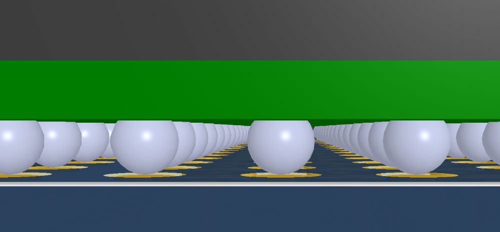
| I don't see any reason that we can't also provide a 'lower detail' model option as part of the generation process. This will not come online immediately, as i'm simply focused on getting the full set of families to come online, but there is no reason it can't be done. For something like a BGA, would you also want all the balls to simply be cylinders? |
Posted By: Nick B
Date Posted: 18 Jun 2013 at 10:13am
|
This is exactly why we have intro pricing now - won't last for long. ------------- Stay connected - follow us! https://twitter.com/PCBLibraries" rel="nofollow - X - http://www.linkedin.com/company/pcb-libraries-inc-/" rel="nofollow - LinkedIn |
Posted By: chrisa_pcb
Date Posted: 18 Jun 2013 at 12:28pm
|
I've played around with the BGA a bit and concerning the pins... balls(sphere) for the BGA are actually the most ideal way of doing this while keeping some definition. Changing them to squares is actually a lot more intensive and produces a file three times the size because it has to generate 6 faces for every pin, rather than 2 iirc. Pretty much the next step lower would be to have a solid cube bound the extents of the pins, and at that point you wouldn't be able to tell if any pins were removed. But since you're simply using low quality for mechanical fit, this may or may not be ok as the area inside of a BGA that has no center pins could feasibly be used for part placement. I guess you could kick it up to high quality at that point if its an issue. |
Posted By: jameshead
Date Posted: 19 Jun 2013 at 12:27am
|
To be honest for something like a BGA or QFN I wouldn't bother with the balls or terminals - I'd just want a square cube. That's all the mechanical guys would be interested in. They are going to be checking the PCB has a single thing against the enclosure - they are not bothered about components under the BGA. Components under the BGA would be my responsibility in the PCB editor and I'd handle this by setting up an area in the BGA footprint with some height restrictions on, so Pulsonix could do the online DRC checking to make sure the components I were fitting there could fit there okay. |
Posted By: Tom H
Date Posted: 19 Jun 2013 at 6:42am
In Altium Designer we like to see the BGA balls. With a 3D mouse ( http://www.3dconnexion.com/products/what-is-a-3d-mouse.html" rel="nofollow - http://www.3dconnexion.com/products/what-is-a-3d-mouse.html ) you can maneuver around to see all the 3D mode component features, solder pad, solder mask, silkscreen and trace routing features. You can visually validate the Footprint to ensure solder joint accuracy. I could easily zoom into the center of the BGA ball pattern and spin around 360 degrees. And you can export the entire PCB and import to SolidWorks for the mechanical engineers. I'm not selling Altium here, I'm simply pointing out some features. ------------- Stay connected - follow us! https://twitter.com/PCBLibraries" rel="nofollow - X - http://www.linkedin.com/company/pcb-libraries-inc-/" rel="nofollow - LinkedIn |
Posted By: jameshead
Date Posted: 19 Jun 2013 at 6:55am
|
Interesting. Pulsonix has a built in 3D viewer in addition to the STEP file preview and output and in Pulsonix I mainly use the built in 3D viewer for a quick check because the STEP file takes longer. I'm not sure how you can visually validate the footprint to ensure solder joint accuracy here since the user is probably going to be outputting the 3D model and the footprint from FPX at the same time so if they've an error input values then it's probably going to be a wrong pitch which would be same on both model and footprint, or the wrong ball diameter. If it's a small error in ball diameter then it looks to me like it may not be noticable, and any large error would probably be seen by the user in FPX or the 2D view of the footprint in the CAD program first. I least that's what I would have thought? I do have a 3Dconnexion space navigator mouse I use at home. It's nice but I need to get some justification first before I can purchase one for me here. The MCAD Engineers each have one of the higher-end 3Dconnexion mice. |
Posted By: dwaltoneng
Date Posted: 19 Jun 2013 at 4:37pm
It looks like it is FreeCAD that is having problems converting the large STEP files. The two converted files that DipTrace won't open, also will not open with FreeWRL. I had a look at the files produced by FreeCAD with a text editor. The two smaller working files are ok, but the files produced for the two larger BGA's are not in VRML format. I still need to find a way to convert from 3D STEP to VRML. |
Posted By: dwaltoneng
Date Posted: 19 Jun 2013 at 5:01pm
Altium is what I am used to. I started using it in the 80's when it was Protel PCB. It used to be a simple low cost program. I have been setting myself up to do work from home, and I thought I would try DipTrace, but I am (not surprisingly) finding some limitations. One limitation is it uses VRML for 3D. Another really annoying problem is you can't do batch updates of footprints. You have to manually reattach the new footprint to every component that uses it. |
Posted By: dwaltoneng
Date Posted: 19 Jun 2013 at 5:07pm
This would be adequate for me at the moment also. Perhaps I might have more luck getting the 3D model into DipTrace. Having the choice of building a high detail or simple model would be great. |
Posted By: dwaltoneng
Date Posted: 14 Jul 2013 at 3:47pm
CAD Exchanger http://www.cadexchanger.com/" rel="nofollow - http://www.cadexchanger.com/ works well converting STEP to VRML. DipTrace has problems with the output of CAD Exchanger, but passing the file through a utility called happy3D (by the user Keith Lee on the DipTrace forum) fixes that. Another method that works but you lose colour information is, open the STEP file with HeeksCAD and save as a STL file, and then convert to vrml using happy3D. |
 chrisa_pcb wrote: