AVX TurboCap Footprint
Printed From: PCB Libraries Forum
Category: PCB Footprint Expert
Forum Name: Questions & Answers
Forum Description: issues and technical support
URL: https://www.PCBLibraries.com/forum/forum_posts.asp?TID=42
Printed Date: 24 Jul 2026 at 4:23pm
Topic: AVX TurboCap Footprint
Posted By: RLS2004
Subject: AVX TurboCap Footprint
Date Posted: 27 Apr 2012 at 11:45am
|
What should the heel, toe and side solder joint dimensions be? AVX Turbo Cap, J style leads, ST205C series High_CV SMPS capacitor. Link to data sheet: http://www.avx.com/docs/Catalogs/turbocap.pdf" rel="nofollow - http://www.avx.com/docs/Catalogs/turbocap.pdf ------------- RLS2004 |
Replies:
Posted By: Tom H
Date Posted: 27 Apr 2012 at 12:12pm
|
You need more than Toe, Heel & Side dimensions to calculate the Pad Size and Spacing. These 7 factors are used to calculate the optimum Land Size Component Body Tolerance – ± 4 Mil (0.1) thru ± 12 (0.3) Also, the "J Style Leads" are really "Outward L Bend" - 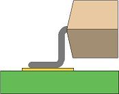 The new upcoming 2012 IPC Footprint Calculator is component lead based to handle every component family. But for the time being here is the info you asked for - Toe = 14 mils (0.35 mm) Heel = 14 mils (0.35 mm) Side = 2 mils (0.05 mm) If you use mils, round-off the pad size and pad center spacing in 1 mil increments. |
Posted By: RLS2004
Date Posted: 27 Apr 2012 at 12:56pm
|
Hi Tom, Thanks for the reply. Did you note that the "J style leads" on this part bend UNDER the component. Looks similar to an SOIC but the leads bend under the part. Old IPC-SM-782 page 10 figure 3-2 shows a "C" bend style of lead that looks similar to this part. What 7351 component family would you recommend for this part? ------------- RLS2004 |
Posted By: Tom H
Date Posted: 27 Apr 2012 at 1:33pm
|
My mistake, but the same solder joint goals for Toe, Heel and Side apply. IPC-7351 uses "Component Families" to break down solder joints. The new IPC Footprint Calculator uses "Component Leads" instead. There are 150 different standard component families and unknown number of non-standard component families, but there are only 21 different Component Lead Styles. What do these Component Families have in common? Ceramic Flat Pack (CFP) Ceramic Quad Flat Pack (CQFP) Small Outline Diode (SOD) Small Outline Transistor (SOT23, SOT223, SOT343 & SOT143) Small Outline Package (SOP) Transistor Outline (TO or DPAK) They all have a Gull Wing lead form. So why apply the same rules to 9 different component families when it's better (more efficient) to apply rules to a single Lead Form. We still have component families in the Footprint Calculator, but the "Preference Rules" are much simpler when the rules are applied to the "Lead Form". |