Adding Minimum Annular Ring for Keepout
Printed From: PCB Libraries Forum
Category: PCB Footprint Expert
Forum Name: Product Suggestions
Forum Description: request new features
URL: https://www.PCBLibraries.com/forum/forum_posts.asp?TID=3527
Printed Date: 05 Jun 2026 at 7:21pm
Topic: Adding Minimum Annular Ring for Keepout
Posted By: m.elsayed
Subject: Adding Minimum Annular Ring for Keepout
Date Posted: 03 Sep 2025 at 7:41am
|
Add a minimum annular ring for keep-out for non-plated holes in 'Tools > Options > Terminals > Through-hole'. The current method of making the non-plated hole keep-out the same size as the Anti-pad does not work it you need a keep-out clearance larger or smaller than the Anti-pad. |
Replies:
Posted By: m.elsayed
Date Posted: 06 Sep 2025 at 11:27pm
| can this feature be added in option file like what be proposed for keep out diameter |
Posted By: Tom H
Date Posted: 07 Sep 2025 at 10:59am
|
Only connectors have non-plated holes. We know you want this to be automatic, but this would force every Footprint Expert user to manually update the Options. Right now it's on automatic per the same size as the Anti-pad and that's the way it's been for the past 20 years. 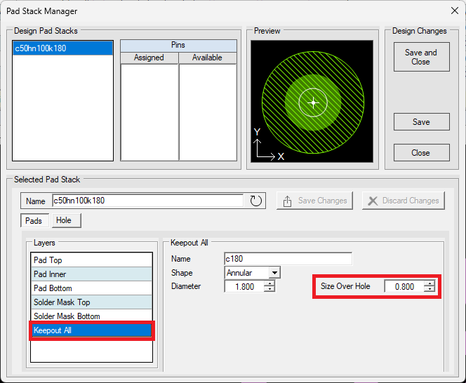 ------------- Stay connected - follow us! https://twitter.com/PCBLibraries" rel="nofollow - X - http://www.linkedin.com/company/pcb-libraries-inc-/" rel="nofollow - LinkedIn |
Posted By: m.elsayed
Date Posted: 07 Sep 2025 at 12:09pm
|
Thanks, Tom i have 2 points 1- not every user need to update option file manually, like any other feature there is default values, so if user doesn't want change default, will leave it with no change, and if user want change , will have ability to change, it will be great idea 2- from shown screen how i control min annular ring, for example if want make it 0.635
|
Posted By: Tom H
Date Posted: 07 Sep 2025 at 1:00pm
|
Making the non-plated keep-out size smaller than the plane anti-pad is not good PCB design practice. Your signal traces need a clean return path on the GND plane. We like to prevent traces from running over a Plane Anti-pad. Your request for this feature was declined based on good PCB design principles and guidelines. ------------- Stay connected - follow us! https://twitter.com/PCBLibraries" rel="nofollow - X - http://www.linkedin.com/company/pcb-libraries-inc-/" rel="nofollow - LinkedIn |