Adding Pin 1 Dot on Assembly Layer
Printed From: PCB Libraries Forum
Category: PCB Footprint Expert
Forum Name: Product Suggestions
Forum Description: request new features
URL: https://www.PCBLibraries.com/forum/forum_posts.asp?TID=3526
Printed Date: 05 Jun 2026 at 7:21pm
Topic: Adding Pin 1 Dot on Assembly Layer
Posted By: m.elsayed
Subject: Adding Pin 1 Dot on Assembly Layer
Date Posted: 03 Sep 2025 at 7:40am
|
Rather than having a chamfer corner for the assembly pin 1 polarity marker. Add a Dot on the assembly layer with required parameters to change the size, height text, line width.
|
Replies:
Posted By: Tom H
Date Posted: 03 Sep 2025 at 9:47am
|
Does anybody else want this feature? Let us know. ------------- Stay connected - follow us! https://twitter.com/PCBLibraries" rel="nofollow - X - http://www.linkedin.com/company/pcb-libraries-inc-/" rel="nofollow - LinkedIn |
Posted By: tgrodnicki
Date Posted: 03 Sep 2025 at 10:50pm
| Some inductors have a dot on their bodies to indicate polarity. That's how I mark it in my footprints. I do this using the Drawing Elements - Symbol/Shapes tool (icon). If this were to be automated, it would also be helpful to have control over the dot's position. |
Posted By: m.elsayed
Date Posted: 04 Sep 2025 at 3:42am
| yes, you correct , this point need to be added it will save more by avoiding do it manual for each part, especially not saved in fpx file( if it done by drawing shapes icon) |
Posted By: Tom H
Date Posted: 04 Sep 2025 at 8:10am
|
Adding Pin 1 Post Assembly Inspection Dots on Silkscreen is automatic. Turn this feature on in Options > Drafting > Silkscreen. ------------- Stay connected - follow us! https://twitter.com/PCBLibraries" rel="nofollow - X - http://www.linkedin.com/company/pcb-libraries-inc-/" rel="nofollow - LinkedIn |
Posted By: tgrodnicki
Date Posted: 04 Sep 2025 at 10:20am
| We are discussing the dot on the Assembly layer and whether it should be added automatically like for the Silkscreen layer. |
Posted By: Tom H
Date Posted: 04 Sep 2025 at 11:34am
|
Do you like the Assembly Polarity Dot better than the Chamfer? Add an Option to switch between the Chamfer or the Dot? Add sizing controls like the Silkscreen Dot for diameter? Where would it go, in the corner of the Assembly Outline (whatever corner pin 1 is) or by Pin 1? How far into the assembly Outline and what about micro footprints? You see how complicated this gets? ------------- Stay connected - follow us! https://twitter.com/PCBLibraries" rel="nofollow - X - http://www.linkedin.com/company/pcb-libraries-inc-/" rel="nofollow - LinkedIn |
Posted By: m.elsayed
Date Posted: 06 Sep 2025 at 11:10pm
|
just you add it as option in Assembly layer, with same parameters as one found in silkscreen layer, without removing chamfer like an new feature
|
Posted By: m.elsayed
Date Posted: 06 Sep 2025 at 11:12pm
|
like reference designator, it found twice one in silkscreen , and other in assmebly layer and user can control any of them, i hope this be like it
|
Posted By: Tom H
Date Posted: 07 Sep 2025 at 7:48am
|
We can't have both the chamfer and the dot. It will have to be one or the other because they will collide with each other in some cases. ------------- Stay connected - follow us! https://twitter.com/PCBLibraries" rel="nofollow - X - http://www.linkedin.com/company/pcb-libraries-inc-/" rel="nofollow - LinkedIn |
Posted By: m.elsayed
Date Posted: 07 Sep 2025 at 12:15pm
|
great, so pleas leave chamfer as default, and give user ability to change it with dot, and have parameter control like one in silkscreen, it will be great if user have ability to choose chamfer or dot in assembly and control dot parameters and a i know , Tom you are a great support for user and try help all of us ,
|
Posted By: m.elsayed
Date Posted: 09 Sep 2025 at 2:58pm
|
Tom, can please check my last reply and let me know your thoughts about that?
|
Posted By: Tom H
Date Posted: 09 Sep 2025 at 3:11pm
|
Your post has received over 4,600 impressions in the past week. We are currently working on adding a new feature for the Pin 1 Assembly Dot. It will have a min/max range so that it can scale per the package body width. It will be located in the corner where Pin 1 is. The current Assembly Polarity Chamfer will be the default setting to match the current output, but the user can change the chamfer to a dot. This new feature will take a couple days to code into the Options file and every user will have to update their Option file by opening and saving it. The next V25.10 pre-release should be available by Monday 9/15/25. ------------- Stay connected - follow us! https://twitter.com/PCBLibraries" rel="nofollow - X - http://www.linkedin.com/company/pcb-libraries-inc-/" rel="nofollow - LinkedIn |
Posted By: m.elsayed
Date Posted: 10 Sep 2025 at 1:50am
|
Great Tom hope to be added with same parameters like one found silkscreen |
Posted By: Tom H
Date Posted: 16 Sep 2025 at 4:14pm
|
The new Assembly Polarity Dot feature has been added to Footprint Expert V25.10 pre-release. Let us know if you like it. To set it up go to - 'Tools > Options > Drafting > Assembly' There are new controls for Min/Max dot sizes. Big footprint get big dots and micro-mini footprints get a small dot. But Chamfer Corner is the program default. ------------- Stay connected - follow us! https://twitter.com/PCBLibraries" rel="nofollow - X - http://www.linkedin.com/company/pcb-libraries-inc-/" rel="nofollow - LinkedIn |
Posted By: m.elsayed
Date Posted: 17 Sep 2025 at 1:38am
| many thanks Tom , for your great support and help |
Posted By: m.elsayed
Date Posted: 18 Sep 2025 at 1:14am
|
Thanks Tom, for adding this as new feature it so great and helpfull
|
Posted By: m.elsayed
Date Posted: 24 Sep 2025 at 7:47am
|
Thanks Tom it is highly appreciated that a dot has been added in the
assembly layer. However, I believe an additional parameter should be
introduced, which becomes active only when the user selects the dot. This
parameter would allow the user to align the dot’s location with that of a
corresponding feature in one of the silkscreen layers
|
Posted By: m.elsayed
Date Posted: 24 Sep 2025 at 5:58pm
|
just if this check added it will be greatful and have more impacts parameter name"align the dot’s location with
as dot the silkscreen layer" will be active only when user select dot option in assembly , and will have 2 values checked or not if check so location should be same , if not checked location like default
|
Posted By: m.elsayed
Date Posted: 24 Sep 2025 at 6:59pm
|
I’m
talking about new one just added polarity do in assembly (Options) , my request
to make it more supportive as explained in our meeting before, give user option
to choose location of it be to same one as in silkscreen , (checked or not checked),
this all |
Posted By: Tom H
Date Posted: 25 Sep 2025 at 8:34am
|
In V25.10 we added a new feature to replace the Assembly Polarity Chamfer with a Dot. V25.10 is the last release this year and we're currently preparing it for the official release next week in October. We might be able to do that in V26 next year. ------------- Stay connected - follow us! https://twitter.com/PCBLibraries" rel="nofollow - X - http://www.linkedin.com/company/pcb-libraries-inc-/" rel="nofollow - LinkedIn |
Posted By: m.elsayed
Date Posted: 25 Sep 2025 at 8:37pm
|
I think this parameter releated for feature added not new feature from scratch Even our discussion shows it requested from start so feature can be helpful
|
Posted By: tgrodnicki
Date Posted: 25 Sep 2025 at 11:14pm
|
The polarity marker on the Silkscreen layer (as it's used for post-assembly inspection) is outside the footprints's outline. For the Assembly layer, I prefer to place the marker inside the outline. If Footprint Expert will have an option to place it in the same location as the dot on the Silkscreen layer, I'll probably never use it.
|
Posted By: Tom H
Date Posted: 26 Sep 2025 at 8:08am
Here is the new Assembly Polarity Dot in a SOP footprint. 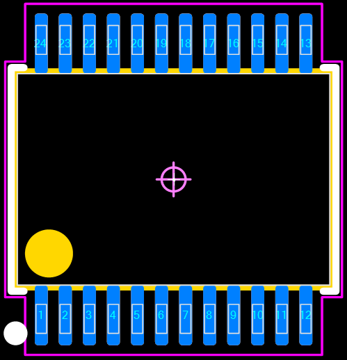 You can select the Minimum / Maximum dot diameter in Assembly > Options. You can toggle between Assembly Chamfer and Dot, whichever you like best. Options are not saved to FPX. Options are automatically applied when you open a footprint. ------------- Stay connected - follow us! https://twitter.com/PCBLibraries" rel="nofollow - X - http://www.linkedin.com/company/pcb-libraries-inc-/" rel="nofollow - LinkedIn |
Posted By: m.elsayed
Date Posted: 28 Sep 2025 at 1:53am
|
great , Thanks, Tom giving user ability to set location of assembly dot same as silkscreen, it will be great, just if checked ok, if not check default value as cahmfer, great control and will help users more
|