Intended Stencil Thickness per IPC Standards
Printed From: PCB Libraries Forum
Category: General
Forum Name: General Discussion
Forum Description: general topics not related to other forums
URL: https://www.PCBLibraries.com/forum/forum_posts.asp?TID=3472
Printed Date: 24 Jul 2026 at 4:23pm
Topic: Intended Stencil Thickness per IPC Standards
Posted By: rweber
Subject: Intended Stencil Thickness per IPC Standards
Date Posted: 20 Feb 2025 at 11:28am
|
Using the IPC standards used by Footprint Expert, is there an intended stencil thickness being considered? Stencil thickness is relevant since it is a factor in the volume of paste deposited, and the aperture area ratio/aspect ratio affecting paste release. For example, I often see example stencil designs on Texas Instruments datasheets that are given for a 0.125mm stencil thickness. |
Replies:
Posted By: Tom H
Date Posted: 20 Feb 2025 at 4:50pm
|
0.125 mm is a standard paste mask stencil thickness. But microminiature footprints might have the stencil thinned to 0.10 mm. IPC-7525C Stencil Design Guidelines is the leading document. Rounded Rectangle apertures help stencil release for lead-free solder alloys. 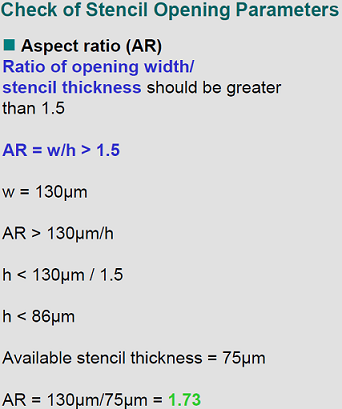 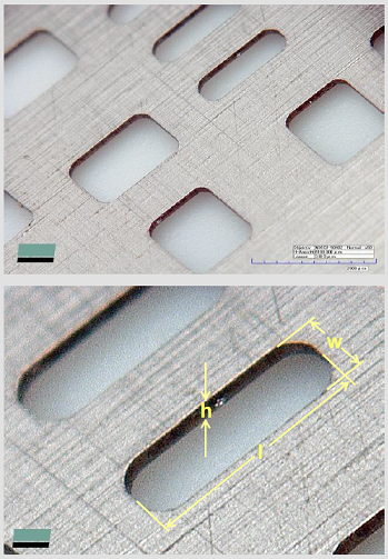 ------------- Stay connected - follow us! https://twitter.com/PCBLibraries" rel="nofollow - X - http://www.linkedin.com/company/pcb-libraries-inc-/" rel="nofollow - LinkedIn |