Silkscreen Polarity Marking Pin 1 Indication
Printed From: PCB Libraries Forum
Category: Libraries
Forum Name: PCB Library Construction Guidelines
Forum Description: Documentation of the Footprint Expert Guidelines
URL: https://www.PCBLibraries.com/forum/forum_posts.asp?TID=3373
Printed Date: 10 Jul 2026 at 11:43pm
Topic: Silkscreen Polarity Marking Pin 1 Indication
Posted By: Tom H
Subject: Silkscreen Polarity Marking Pin 1 Indication
Date Posted: 07 Apr 2024 at 3:02pm
|
Polarity Marking not necessary for packages that can be inverted during assembly (like a resistor). The minimum Dot diameter should be 0.40 mm. Anything smaller is too hard to see during the Post Assembly Inspection process. The range for Dot sizes is 0.40 – 1.00. The Dot diameter should be the same value as the pad width but keep it within the range. A dot is normally used, but other symbols like square and triangle can be used. On very dense part placement boards, a line drawn the length of pin 1 can be used, but it's hard to identify it as a pin 1 polarity marker. 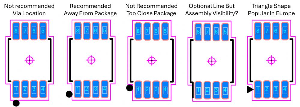 ------------- Stay connected - follow us! https://twitter.com/PCBLibraries" rel="nofollow - X - http://www.linkedin.com/company/pcb-libraries-inc-/" rel="nofollow - LinkedIn |
Replies:
Posted By: Tom H
Date Posted: 07 Apr 2024 at 3:06pm
|
The Assembly Outline is a closed polygon with an assembly reference designator inside it. 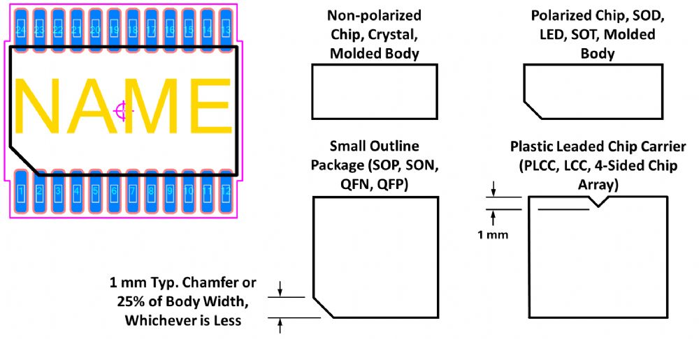 ------------- Stay connected - follow us! https://twitter.com/PCBLibraries" rel="nofollow - X - http://www.linkedin.com/company/pcb-libraries-inc-/" rel="nofollow - LinkedIn |
Posted By: Tom H
Date Posted: 07 Apr 2024 at 3:09pm
Connector Polarity Marking general guidelines. 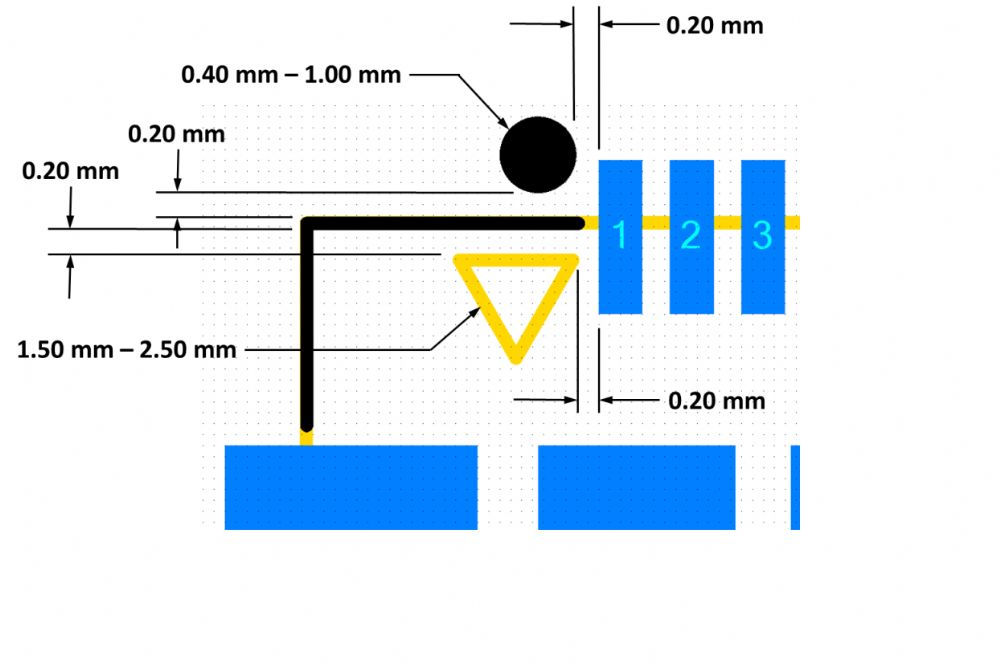 ------------- Stay connected - follow us! https://twitter.com/PCBLibraries" rel="nofollow - X - http://www.linkedin.com/company/pcb-libraries-inc-/" rel="nofollow - LinkedIn |