Counter-Clockwise Pad Numbering?
Printed From: PCB Libraries Forum
Category: PCB Footprint Expert
Forum Name: Questions & Answers
Forum Description: issues and technical support
URL: https://www.PCBLibraries.com/forum/forum_posts.asp?TID=3031
Printed Date: 24 Jul 2026 at 9:19pm
Topic: Counter-Clockwise Pad Numbering?
Posted By: Blaylock
Subject: Counter-Clockwise Pad Numbering?
Date Posted: 07 Jan 2022 at 9:57am
|
I'm a total noob with FPExp 2022. I'm trying to build a pattern with Counter-Clockwise numbered pads. (PDIP-6 On Semi B46BY) Using the Pin Array Wizard there seems to be no selectable Step pattern that will result in this numbering scheme. All of the available options result in interdigitated (Connector Like) numberings. Am I missing something, or just pushing a boulder up-hill? |
Replies:
Posted By: Tom H
Date Posted: 07 Jan 2022 at 10:13am
|
All footprints have counterclockwise pin numbers. We cannot find Onsemi P/N B46BY. Can you provide a web-link to the datasheet? Or post a picture of the package with the pin numbers. Or attach a FPX file in a .zip file. Thanks ------------- Stay connected - follow us! https://twitter.com/PCBLibraries" rel="nofollow - X - http://www.linkedin.com/company/pcb-libraries-inc-/" rel="nofollow - LinkedIn |
Posted By: Blaylock
Date Posted: 07 Jan 2022 at 10:42am
|
Sorry, 646BY is the On-Semi Case Code. It's a standard pattern: https://www.onsemi.com/pdf/datasheet/4n37m-d.pdf" rel="nofollow - https://www.onsemi.com/pdf/datasheet/4n37m-d.pdf I think a similar part is in the POD under MOC3041 I can manually re-number the pads, but there doesn't seem to be a way to auto-generate them, numbered down the left side, then up the right side. |
Posted By: Blaylock
Date Posted: 07 Jan 2022 at 11:10am
|
I took a screenshot of what I'm seeing: https://drive.google.com/file/d/1lXyacAkYd_kpptmkN44PQdujj5TdP4wx/view?usp=sharing" rel="nofollow - https://drive.google.com/file/d/1lXyacAkYd_kpptmkN44PQdujj5TdP4wx/view?usp=sharing
|
Posted By: Tom H
Date Posted: 07 Jan 2022 at 11:16am
|
This is the PDIP6 in V2022.01 Footprint Expert through-hole calculator. What is the problem? 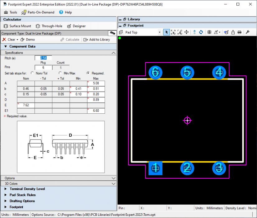 ------------- Stay connected - follow us! https://twitter.com/PCBLibraries" rel="nofollow - X - http://www.linkedin.com/company/pcb-libraries-inc-/" rel="nofollow - LinkedIn |
Posted By: Tom H
Date Posted: 07 Jan 2022 at 11:27am
|
You can use the Through-hole DIP component family to create the pattern and then move it to FP Designer to swap out the pad stacks with SMD pads. ------------- Stay connected - follow us! https://twitter.com/PCBLibraries" rel="nofollow - X - http://www.linkedin.com/company/pcb-libraries-inc-/" rel="nofollow - LinkedIn |
Posted By: Blaylock
Date Posted: 07 Jan 2022 at 12:11pm
|
Thanks Tom. I see now that both the Surface Mount and Through-Hole calculators automatically generate a counter-clockwise numbering scheme. I've made TH and SM patterns and put them into the Demo Library. When I "View" the selected part or footprint it opens into the calculator used to generate it.... Per your reply how can I "import" a footprint into the Designer for editing? This Works, I found the "Move Footprint to Designer" toolbar icon in the Footprint window. It is unfortunate that the Designer doesn't automagically do the "right thing" for making ICs. I do like the custom part naming options that the Designer also allows, but would like choice of applied separator. "-" vs "_" I'm unstuck..... Thanks for the fast replies. +Paul |
Posted By: Tom H
Date Posted: 07 Jan 2022 at 1:11pm
|
We need to do a webcast to see what you are doing. There are no limitations to pin assignments in FP Designer. Enter the coordinate of Pin 1 and the Step is how many more pins you need, and the Pitch is either negative or positive value. Negative value the pin assignments go clockwise and Positive is counterclockwise. All Footprint Expert users have unlimited technical support, so we can do a FP Designer demo to show you all the features. ------------- Stay connected - follow us! https://twitter.com/PCBLibraries" rel="nofollow - X - http://www.linkedin.com/company/pcb-libraries-inc-/" rel="nofollow - LinkedIn |
Posted By: Tom H
Date Posted: 07 Jan 2022 at 1:33pm
There's an icon button in the toolbar that allows you to move most footprints from the Calculator to FP Designer. 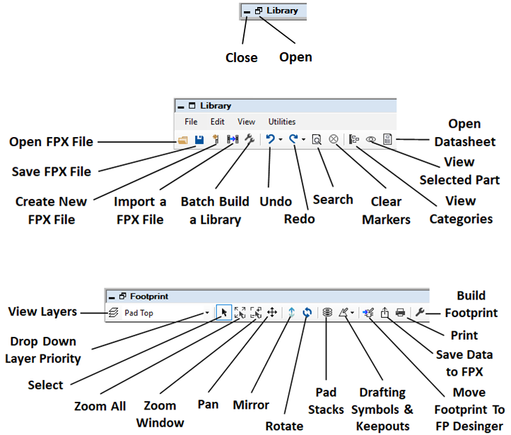 ------------- Stay connected - follow us! https://twitter.com/PCBLibraries" rel="nofollow - X - http://www.linkedin.com/company/pcb-libraries-inc-/" rel="nofollow - LinkedIn |