The pad size in the terminal density level 'L'
Printed From: PCB Libraries Forum
Category: PCB Footprint Expert
Forum Name: Questions & Answers
Forum Description: issues and technical support
URL: https://www.PCBLibraries.com/forum/forum_posts.asp?TID=2949
Printed Date: 25 Jul 2026 at 6:33am
Topic: The pad size in the terminal density level 'L'
Posted By: diverger
Subject: The pad size in the terminal density level 'L'
Date Posted: 06 Jul 2021 at 8:51pm
|
Today, I use the 2021.09 version to generate a SC89 footprint (using the SOFL package). I found the pad size in 'L' density is generated according to the nominal size. Assuming a pin with such width specification: MIN = 0.23, NOM = 0.28, MAX = 0.33 Then the pad width generated is 0.28. Is it designed like this, or it's a bug? Thanks.
|
Replies:
Posted By: Tom H
Date Posted: 06 Jul 2021 at 9:50pm
|
You would have to send us an email with a FPX file attached with a step by step instruction to reproduce a bug. Are you using the default solder joint goals and mfr. tolerances and package tolerances? Lots of questions. I have a datasheet. Would that work? https://www.vishay.com/docs/71612/sc89_6leads.pdf" rel="nofollow - https://www.vishay.com/docs/71612/sc89_6leads.pdf ------------- Stay connected - follow us! https://twitter.com/PCBLibraries" rel="nofollow - X - http://www.linkedin.com/company/pcb-libraries-inc-/" rel="nofollow - LinkedIn |
Posted By: diverger
Date Posted: 06 Jul 2021 at 11:20pm
Yes, I use the default solder joint goals and mfr, etc. The datasheet of the part is https://www.onsemi.com/pdf/datasheet/nta4153n-d.pdf" rel="nofollow - https://www.onsemi.com/pdf/datasheet/nta4153n-d.pdf , the SC-89 package.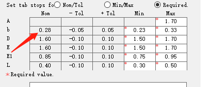 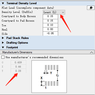  |
Posted By: Tom H
Date Posted: 07 Jul 2021 at 9:00am
|
It's perfect. The pad width can not be any smaller than the nominal lead width. ------------- Stay connected - follow us! https://twitter.com/PCBLibraries" rel="nofollow - X - http://www.linkedin.com/company/pcb-libraries-inc-/" rel="nofollow - LinkedIn |
Posted By: diverger
Date Posted: 07 Jul 2021 at 5:49pm
|
I thought the pad should be equal or greater than the max. specification. Now if the pad is generated as nominal width. we must rely on the courtyard to make sure the pad won't get connected with other, right? Thanks.
|
Posted By: Tom H
Date Posted: 07 Jul 2021 at 9:09pm
|
Not in the "Least Density Level". Least = minimum pad size, but still functional and manufacturable. Use Nominal Density or change the "Tools > Options > Terminals > Surface Mount > Flat Lead > Least > Side" You have the controls to create your PCB library. 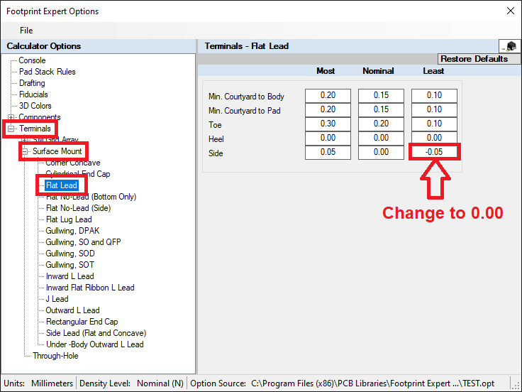 ------------- Stay connected - follow us! https://twitter.com/PCBLibraries" rel="nofollow - X - http://www.linkedin.com/company/pcb-libraries-inc-/" rel="nofollow - LinkedIn |