Pad to Pad space in 3-pin SOFL
Printed From: PCB Libraries Forum
Category: PCB Footprint Expert
Forum Name: Questions & Answers
Forum Description: issues and technical support
URL: https://www.PCBLibraries.com/forum/forum_posts.asp?TID=2836
Printed Date: 25 Jul 2026 at 6:18am
Topic: Pad to Pad space in 3-pin SOFL
Posted By: Batiskaff
Subject: Pad to Pad space in 3-pin SOFL
Date Posted: 03 Mar 2021 at 2:47am
|
In Rules "Pad to Pad" spacing = 0.15mm But pads were trimmed and now Pad1 to Pad2 space=0.33mm 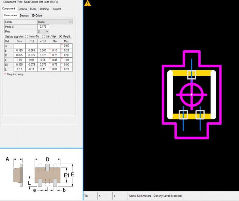 |
Replies:
Posted By: Tom H
Date Posted: 03 Mar 2021 at 10:08am
|
The Pad Stack Rules are intended for medium to large packages. You can't have a pin pitch of 0.175 when the maximum lead thickness is 0.23. That's impossible. Turn the minimum pad to pad off for micro-miniature packages. The pin pitch is 0.175. This can't be true. The pin pitch is between the Center of the Body and the center of the pin. You need to double to pin pitch to 0.35 mm. But I would also change the solder joint goals downward slightly. Please provide a link to the datasheet URL. ------------- Stay connected - follow us! https://twitter.com/PCBLibraries" rel="nofollow - X - http://www.linkedin.com/company/pcb-libraries-inc-/" rel="nofollow - LinkedIn |
Posted By: Batiskaff
Date Posted: 03 Mar 2021 at 11:53am
|
Component DSCQ001: https://www.digikey.be/htmldatasheets/production/770431/0/0/1/dscq001.html" rel="nofollow - https://www.digikey.be/htmldatasheets/production/770431/0/0/1/dscq001.html
|
Posted By: Tom H
Date Posted: 03 Mar 2021 at 12:13pm
|
This package in not a SOTFL. The SOTFL component family has the Terminal Lead Width the same size for all leads. This JEITA-SC-1168B case code is none standard and must use the mfr. recommended footprint. Package: 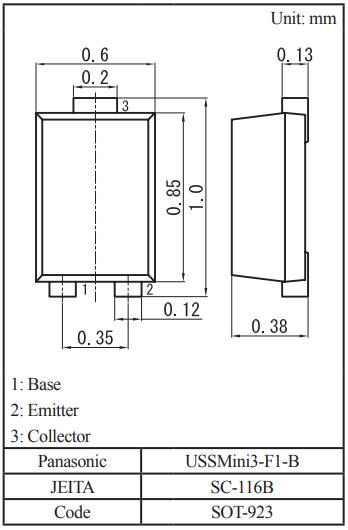 Mfr. Recommended footprint: 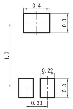 ------------- Stay connected - follow us! https://twitter.com/PCBLibraries" rel="nofollow - X - http://www.linkedin.com/company/pcb-libraries-inc-/" rel="nofollow - LinkedIn |