Solder Mask Oversize?
Printed From: PCB Libraries Forum
Category: PCB Footprint Expert
Forum Name: Questions & Answers
Forum Description: issues and technical support
URL: https://www.PCBLibraries.com/forum/forum_posts.asp?TID=2208
Printed Date: 25 Jul 2026 at 12:45pm
Topic: Solder Mask Oversize?
Posted By: Kenji
Subject: Solder Mask Oversize?
Date Posted: 03 Sep 2017 at 10:32pm
|
I usually use FP Designer. Then I have a question regarding the corner chamfer. The component picture has the solder mask oversize 0.05 mm equally.  I edited the pad stack to use the chamfer feature. But but how do you make the solder mask oversize 0.05 mm equally? 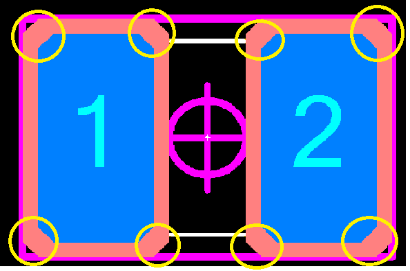 |
Replies:
Posted By: Tom H
Date Posted: 04 Sep 2017 at 6:09am
|
In FP Designer you can edit the full pad stack (Top, Solder Mask and Paste Mask" in "Pad Stack Manager". Select the layer you want to edit and change the values for both the Top and Solder Mask separately. Note: the solder mask chamfer will be slightly larger than the Top pad. Let us know if you need a webcast training session and we'll set it up immediately. ------------- Stay connected - follow us! https://twitter.com/PCBLibraries" rel="nofollow - X - http://www.linkedin.com/company/pcb-libraries-inc-/" rel="nofollow - LinkedIn |
Posted By: Kenji
Date Posted: 04 Sep 2017 at 5:44pm
|
I knew. I use the pad stack manager. But The program has only a Chamfer's length. All I want to do is to have a gap between Top and Solder Mask Top.
|
Posted By: Tom H
Date Posted: 04 Sep 2017 at 6:01pm
|
Unfortunately, you have to figure out the solder mask chamfer size for the solder mask layer. 0.05 mm pad chamfer = 0.075 mm solder mask chamfer to keep the 0.05 mm oversize. Or you can create a new pad stack in the "Pad Stack Designer" with a 0.05 mm solder mask over size and it will auto-calculate a new pad stack. Then swap out the pin numbers with the new pad stack in the "Pad Stack Manager". ------------- Stay connected - follow us! https://twitter.com/PCBLibraries" rel="nofollow - X - http://www.linkedin.com/company/pcb-libraries-inc-/" rel="nofollow - LinkedIn |
Posted By: Kenji
Date Posted: 04 Sep 2017 at 6:59pm
|
Thanks. 0.05 mm pad chamfer = 0.075 mm solder mask chamfer to keep the 0.05 mm oversize. This is good idea. The other idea about creating a new pad stack in Pad Stack Designer is unsatisfactory, because It creates a 0.10 mm solder mask chamfer and the annular area is narrower than 0.05 mm.
|
Posted By: Tom H
Date Posted: 07 Sep 2017 at 9:34am
|
We fixed this FP Designer Chamfered Pad Solder Mask issue and re-released V2017.17. Try the updated version. ------------- Stay connected - follow us! https://twitter.com/PCBLibraries" rel="nofollow - X - http://www.linkedin.com/company/pcb-libraries-inc-/" rel="nofollow - LinkedIn |
Posted By: NoellEagan
Date Posted: 19 Oct 2017 at 9:54am
|
Hi, I am a new user here. As per my knowledge in FP Designer you can edit the full pad stack (Top, Solder Mask and Paste Mask) in "Pad Stack Manager". Also you should select the layer you want to edit and change the values for both the Top and Solder Mask separately. |