Calculator to FP Designer
Printed From: PCB Libraries Forum
Category: PCB Footprint Expert
Forum Name: Questions & Answers
Forum Description: issues and technical support
URL: https://www.PCBLibraries.com/forum/forum_posts.asp?TID=2101
Printed Date: 06 Jun 2026 at 12:20am
Topic: Calculator to FP Designer
Posted By: jnshah
Subject: Calculator to FP Designer
Date Posted: 04 Mar 2017 at 1:11pm
I created SHDRRA14W50P200_100_14X1_2990X760H280. The resulting decal in PADS has silkscreen in multiple overlapping segments. The invisible part is only 0.025 thick, the visible parts (multiple segments) are 0.12 thick and they all overlap. Here is a screen shot with the assembly layer disabled. Is this expected?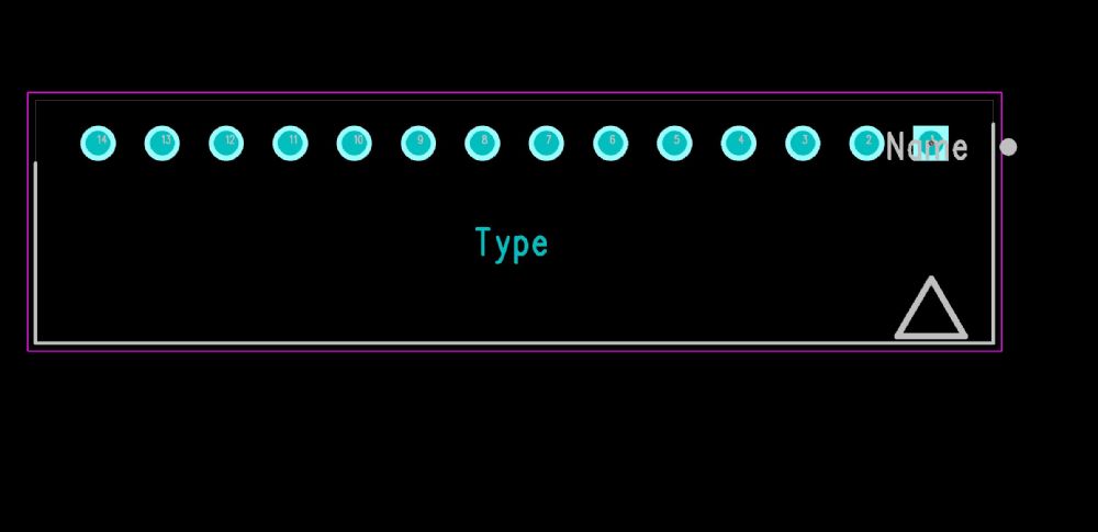 |
Replies:
Posted By: jnshah
Date Posted: 04 Mar 2017 at 1:13pm
| This is version 2010.10 PRE6. |
Posted By: jnshah
Date Posted: 04 Mar 2017 at 1:25pm
| It is the same with 2010.08 and so may be this is expected. I will appreciate if you can help me understand why the silkscreen is not a complete rectangle as one would expect, given the clearances. |
Posted By: Jeff.M
Date Posted: 04 Mar 2017 at 1:45pm
|
Can you send us an fpx library file containing this part? ------------- Stay connected - follow us! https://twitter.com/PCBLibraries" rel="nofollow - X - http://www.linkedin.com/company/pcb-libraries-inc-/" rel="nofollow - LinkedIn |
Posted By: jnshah
Date Posted: 04 Mar 2017 at 2:11pm
|
Sure. Here it is attached. uploads/11567/test_srdhdr.fpx" rel="nofollow - uploads/11567/test_srdhdr.fpx Also, please note that when I create a new part, it shows up as the following with the silkscreen as an incomplete rectangle (This is 2017.08). 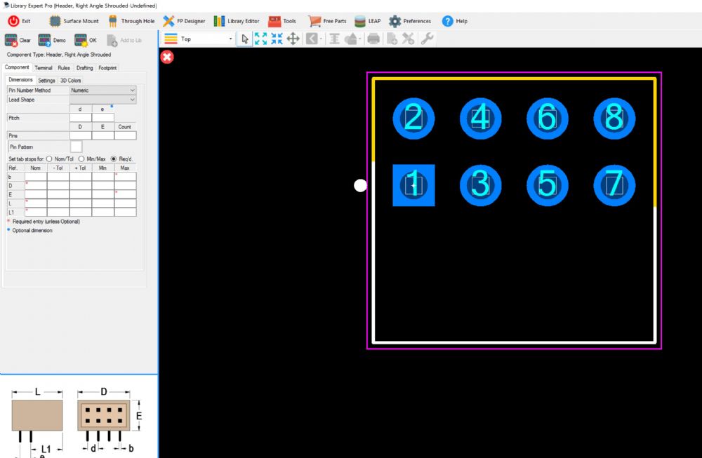 |
Posted By: Jeff.M
Date Posted: 04 Mar 2017 at 3:08pm
|
The auto-generated silkscreen outline isn't designed to create a rectangle. ------------- Stay connected - follow us! https://twitter.com/PCBLibraries" rel="nofollow - X - http://www.linkedin.com/company/pcb-libraries-inc-/" rel="nofollow - LinkedIn |
Posted By: jnshah
Date Posted: 04 Mar 2017 at 3:26pm
|
Jeff, Thank you. Can you please clarify, do you mean it is designed to create an asymmetrical C shape as shown or is it designed to create a rectangular boundary with individual segments? Thank you.
|
Posted By: jnshah
Date Posted: 04 Mar 2017 at 3:49pm
|
I think I get it. You generate a C shape. As my preferences are set to generate pin 1 line indicator, that makes it asymmetrical. I need a fully enclosed rectangle. I used the FP designer to create one. All set. Thank you.
|
Posted By: Tom H
Date Posted: 04 Mar 2017 at 4:25pm
|
You can create the original footprint in the Calculator to use the automation and it creates a great 3D STEP model. Save to FPX and replace the Physical Description for the Calculator part and put "3D STEP Model". Then push the part from the Calculator into FP Designer to touch up the drafting details and save to FPX. We use this technique a lot. Watch this video - http://www.pcblibraries.com/products/fpx/userguide/default.asp?ch=7.6" rel="nofollow - http://www.pcblibraries.com/products/fpx/userguide/default.asp?ch=7.6 You can do this with any Calculator part. ------------- Stay connected - follow us! https://twitter.com/PCBLibraries" rel="nofollow - X - http://www.linkedin.com/company/pcb-libraries-inc-/" rel="nofollow - LinkedIn |
Posted By: jnshah
Date Posted: 04 Mar 2017 at 5:59pm
| Thank you both, Tom and Jeff. This has been incredibly helpful. Sorry for creating unnecessary alarm over the weekend. |