Pad Stack Manager
Printed From: PCB Libraries Forum
Category: PCB Footprint Expert
Forum Name: Questions & Answers
Forum Description: issues and technical support
URL: https://www.PCBLibraries.com/forum/forum_posts.asp?TID=1992
Printed Date: 05 Jun 2026 at 12:07pm
Topic: Pad Stack Manager
Posted By: BennsPCB
Subject: Pad Stack Manager
Date Posted: 03 Nov 2016 at 4:09am
|
I'm creating a 4-pin SIP Hall sensor (Allegro A1363) FP and want to increase pad clearance by using an oblong pad instead of a round one, but Pad Stack Manager won't let me do that. Why? Cheers, ... 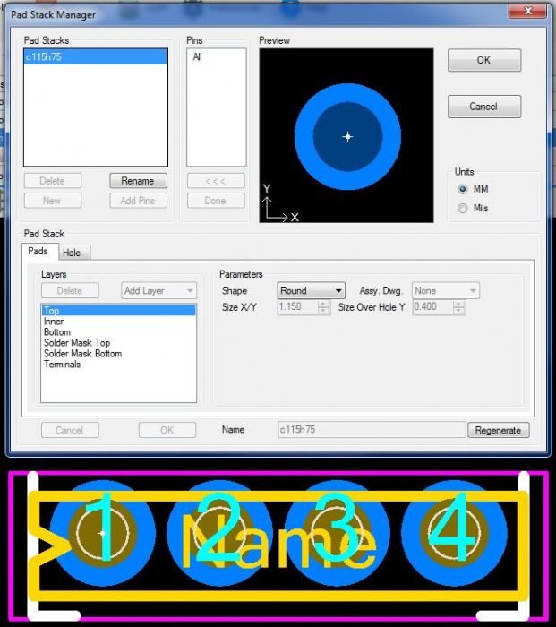 |
Replies:
Posted By: Tom H
Date Posted: 03 Nov 2016 at 7:04am
|
You Must create this part in FP Designer. The Calculator does not have a Oblong Through-hole pad stack option. ------------- Stay connected - follow us! https://twitter.com/PCBLibraries" rel="nofollow - X - http://www.linkedin.com/company/pcb-libraries-inc-/" rel="nofollow - LinkedIn |
Posted By: BennsPCB
Date Posted: 03 Nov 2016 at 7:21am
|
OK Tom , I see. But, it seems like a 2-stage takeoff. May I request a button that takes me to FP Designer directly (with the data already created)? And I still want to name it acc. to IPC-std. Perhaps with a note/naming that user defined padstack is used. Cheers, ... |
Posted By: Tom H
Date Posted: 03 Nov 2016 at 7:29am
|
There is a button to move your Calculator part to FP Designer. However, these component families will not transfer - DPAK, TO220, TO92, Mounting Holes, Aluminum
Electrolytic Capacitor. 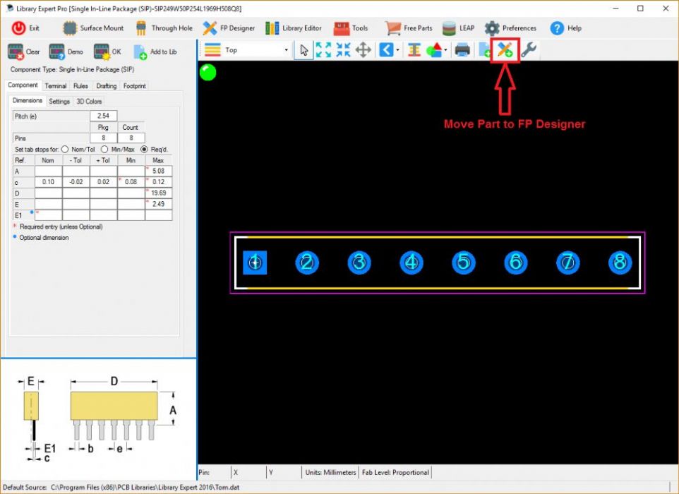 ------------- Stay connected - follow us! https://twitter.com/PCBLibraries" rel="nofollow - X - http://www.linkedin.com/company/pcb-libraries-inc-/" rel="nofollow - LinkedIn |
Posted By: BennsPCB
Date Posted: 03 Nov 2016 at 7:37am
|
Tried that, but all data except the pins disappeared. Not very useful. |
Posted By: Tom H
Date Posted: 03 Nov 2016 at 7:43am
|
Did you select the "Body" tab and enter the package dimensions? 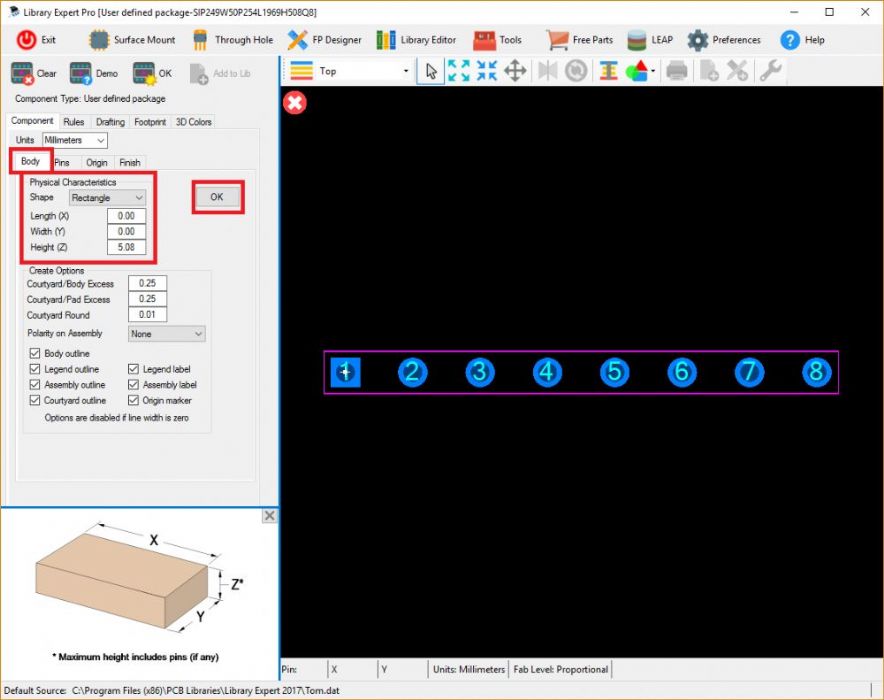 ------------- Stay connected - follow us! https://twitter.com/PCBLibraries" rel="nofollow - X - http://www.linkedin.com/company/pcb-libraries-inc-/" rel="nofollow - LinkedIn |
Posted By: BennsPCB
Date Posted: 03 Nov 2016 at 8:21am
|
Nope, I came from Through Hole/Single In-Line Package (SIP), where I have entered all my data. It's from here it would be useful to enter the FP Designer. (with data intact)  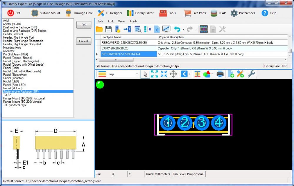 |
Posted By: Tom H
Date Posted: 03 Nov 2016 at 8:38am
|
OK, this is a bug and we're going to release V2016.14 later today. In the meantime, you can create that 4-pin SIP in FP Designer with Oblong PTH pad stacks in less than 3 minutes. Thank you for reporting this issue. ------------- Stay connected - follow us! https://twitter.com/PCBLibraries" rel="nofollow - X - http://www.linkedin.com/company/pcb-libraries-inc-/" rel="nofollow - LinkedIn |
Posted By: BennsPCB
Date Posted: 03 Nov 2016 at 8:47am
OK, nice  Cheers, ... |
Posted By: Nick B
Date Posted: 03 Nov 2016 at 4:27pm
|
2016.14 is online in our Downloads section, please run it and let us know. ------------- Stay connected - follow us! https://twitter.com/PCBLibraries" rel="nofollow - X - http://www.linkedin.com/company/pcb-libraries-inc-/" rel="nofollow - LinkedIn |
Posted By: BennsPCB
Date Posted: 04 Nov 2016 at 12:23am
|
Hi Nick. Seems working, but why is the label always turned 270 deg. and max sized? Cheers, ... |
Posted By: Tom H
Date Posted: 04 Nov 2016 at 8:51am
|
The Ref Des Label is 270 deg. so that the Name starts at the Bottom and goes to the top. If the Label was 90 deg. the Name would start at the top. Maybe we'll put in a Preference to allow the user to select the Ref Des Label rotation. ------------- Stay connected - follow us! https://twitter.com/PCBLibraries" rel="nofollow - X - http://www.linkedin.com/company/pcb-libraries-inc-/" rel="nofollow - LinkedIn |