Via Fanout For BGA
Printed From: PCB Libraries Forum
Category: PCB Footprint Expert
Forum Name: Questions & Answers
Forum Description: issues and technical support
URL: https://www.PCBLibraries.com/forum/forum_posts.asp?TID=1888
Printed Date: 24 Jul 2026 at 9:42pm
Topic: Via Fanout For BGA
Posted By: mahmoodv99
Subject: Via Fanout For BGA
Date Posted: 10 May 2016 at 10:38pm
|
Add option to add fan out for BGA in footprint itself with options via size, trace size, etc. 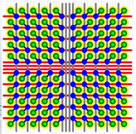
|
Replies:
Posted By: Tom H
Date Posted: 15 May 2016 at 9:13am
|
This feature is better to do in the CAD tool. Many CAD tools have automatic via fanout and if it doesn't, you need to ask the CAD vendor to add that feature into the CAD tool. Vias in a PCB Footprint library part become Pins and the BGA pad and via connecting line become Associated Copper. This makes the library part size very big. We tried this once and spent a lot of time creating it, but it was a disaster. It sounds like a good idea, but you should manually try to do it and put the resulting part in a PCB layout to test it. Then you will see that it's impossible to fanout BGA's in the library part. Also, most BGA's have unused pins and if those pins have vias, it blocks routing channels and bottom side capacitor placement. ------------- Stay connected - follow us! https://twitter.com/PCBLibraries" rel="nofollow - X - http://www.linkedin.com/company/pcb-libraries-inc-/" rel="nofollow - LinkedIn |