

|
|
Pin1 / Package marking |
Post Reply 
|
| Author | |
Luke 
Active User 

Joined: 24 Jan 2013 Location: Drammen, Norway Status: Offline Points: 12 |
 Post Options Post Options
") Thanks(0) Thanks(0)
 Quote Reply Quote Reply
 Topic: Pin1 / Package marking Topic: Pin1 / Package markingPosted: 06 May 2015 at 11:16pm |
|
Hello.
I have a package that has the markings on pin 4 and NOT pin 1. Is there a way to change "pin 1" to another pin, say 4? Regards, Luke 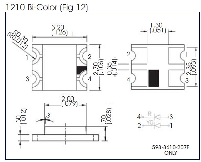 |
|
 |
|

|
|
|
|
|
Tom H
Admin Group 

Joined: 05 Jan 2012 Location: San Diego, CA Status: Offline Points: 6070 |
Post Options
Thanks(0)
Quote Reply
Posted: 07 May 2015 at 9:12am |
|
You should be using the "Side Concave Package (2, 4 pins) component family.
You can select any Pin and RMB > Reorder pins. But it looks like the default pin assignment matches the default calculator pin assignment. 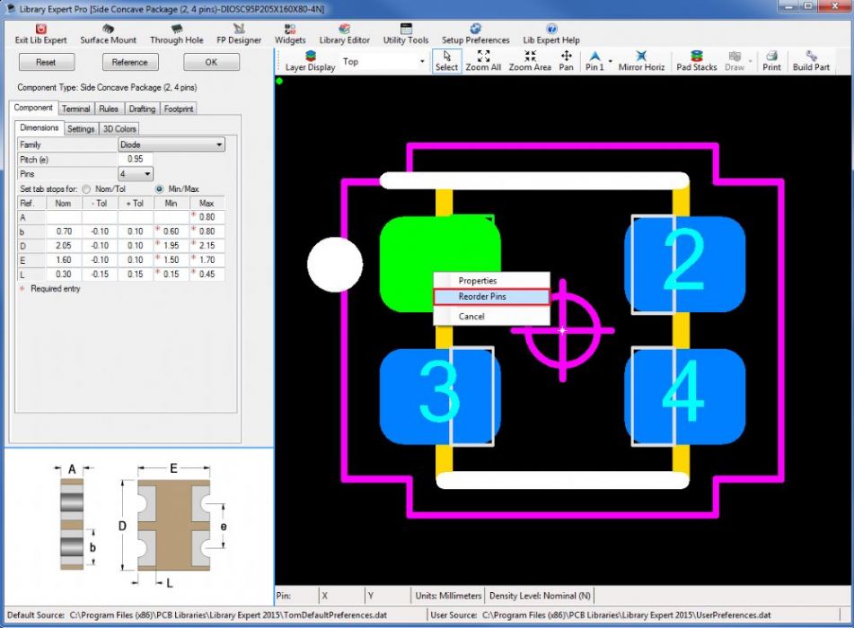 |
|
|
|
|
Post Reply
|
|
| Tweet |
| Forum Jump | Forum Permissions You cannot post new topics in this forum You cannot reply to topics in this forum You cannot delete your posts in this forum You cannot edit your posts in this forum You cannot create polls in this forum You cannot vote in polls in this forum |


 Topic Options