
 |

|
Minimum Solder Mask Web & Gang Mask |
Post Reply 
|
| Author | |
Nick B 
Admin Group 

Joined: 02 Jan 2012 Status: Offline Points: 1996 |
 Post Options Post Options
 Thanks(0) Thanks(0)
 Quote Quote  Reply Reply
 Topic: Minimum Solder Mask Web & Gang Mask Topic: Minimum Solder Mask Web & Gang MaskPosted: 09 Jan 2025 at 7:22pm |
|
The fabrication process has its minimum rules for features in the PCB layout. Some of the Minimum Feature Rules depend on each fab shop (Note: all values are in millimeters)
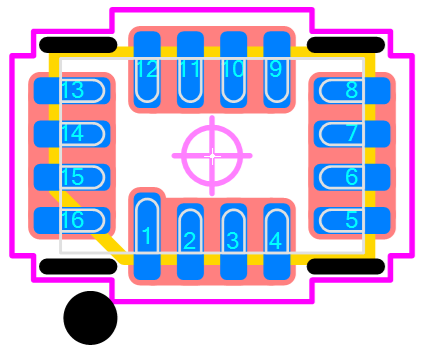
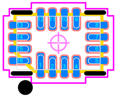
In this article we will focus on the minimum solder mask web (sliver) and gang masking. The solder mask swell sizes range from 0.05 – 0.10, but in a typical CAD library, all the solder mask swell sizes are the same value for consistency. If you use a 0.05 solder mask swell for footprint creation, the same rule applies to every footprint in the CAD library. The typical minimum pad to pad spacing is 0.15. If the solder mask swell is 0.05, this will create a 0.05 solder mask web (sliver). The minimum solder mask web is 0.075. A 0.05 web violates the minimum requirement. In this case, the entire row of pads will be gang masked to prevent a rule violation. It is a common myth that gang masking a row of pads could potentially cause solder bridging between pads that have a 0.15 minimum spacing rule. However, solder mask and prepreg are both epoxy resins. Solder will not stick to regular epoxy resin because epoxy is a non-conductive material that doesn't readily melt or bond with the solder at soldering temperatures. Here is a 0.40 pin pitch QFN with a 0.05 solder mask swell. The pad width is 0.25. The minimum pad to pad rule is 0.15. The 0.75 minimum solder mask web was violated causing Footprint Expert to gang mask the rows. Note: if you create a PCB footprint with a solder mask swell that violates the fabrication shop minimum web, the manufacturer will automatically gang mask the row of pads without your approval (if it’s a fast turn prototype). If the PCB is going to production, a fabrication CAM DRC check will flag all solder mask violations when the minimum solder mask web is not met. The DRC check results will be sent to the PCB designer to fix all the minimum rule violations. Also, if any silkscreen violates the solder mask opening, fabrication will automatically trim all silkscreen outlines that violate that rule. Gang Masked Pads with no solder mask web:  However, you can change the minimum pad to pad spacing rule to 0.175 to accommodate a 0.05 solder mask swell and a 0.075 web. Changing the minimum pad to pad to 0.175 will change the pad width to 0.225. The nominal terminal width is 0.20. Non-Gang Masked Pads with solder mask web:  If you desire to have a solder mask web in-between every pad, do this math to achieve it. Solder Mask Swell x 2 + Minimum Solder Mask Web = Minimum Pad to Pad Spacing. Robust Example: SM Swell of 0.75 x 2 = 0.150 + Min. SM Web = 0.10 = 0.25 Min. Pad to Pad. Looking forward to the day that the fabrication process can manufacture a 0.05 solder mask web. Then, if the solder mask swell is 0.05 and the minimum pad to pad is 0.15 the solder mask web will be 0.05 and every pad on the PCB layout will have a solder mask web. Wishful thinking. The solder mask swell is important for DFM because applying the solder mask requires slop tolerances and the minimum solder mask swell could vary from one manufacturer to another. Many PCB designers create PCB library parts with a solder mask 1:1 scale of the pad size. Then they allow the fabrication shop to swell the solder mask to meet the fabrication shop minimum solder mask swell. This concept allows the PCB to meet DFM requirements for every manufacturer.  PCB Footprint Expert Simplify your PCB design process with the Footprint Expert, the ultimate tool for automating solder mask calculations and creation. It ensures your layouts meet fabrication rules like minimum solder mask web and swell, preventing design rule violations and reducing the need for manual adjustments. With the Footprint Expert, you can optimize pad spacing, manage gang masking, and maintain DFM compliance with ease. Let the Footprint Expert handle both complexities and nuances so you can focus on creating flawless PCB designs faster and more efficiently! Get your FREE Footprint Calculator or Footprint Expert Evaluation License: Call: 847-557-2300 |
|
 |
|

|
|
 |
|
Post Reply 
|
|
| Tweet |
| Forum Jump | Forum Permissions  You cannot post new topics in this forum You cannot reply to topics in this forum You cannot delete your posts in this forum You cannot edit your posts in this forum You cannot create polls in this forum You cannot vote in polls in this forum |