

|
|
How To Genereate CAPAE Footprint? |
Post Reply 
|
| Author | |
Sujith 
Active User 
Joined: 12 Sep 2016 Status: Offline Points: 22 |
 Post Options Post Options
") Thanks(1) Thanks(1)
 Quote Reply Quote Reply
 Topic: How To Genereate CAPAE Footprint? Topic: How To Genereate CAPAE Footprint?Posted: 12 Sep 2016 at 6:23am |
|
Hi,
I am new to this tool. I was trying to generate a footprint foor SMD Aluminium Capacitorm but no success ! 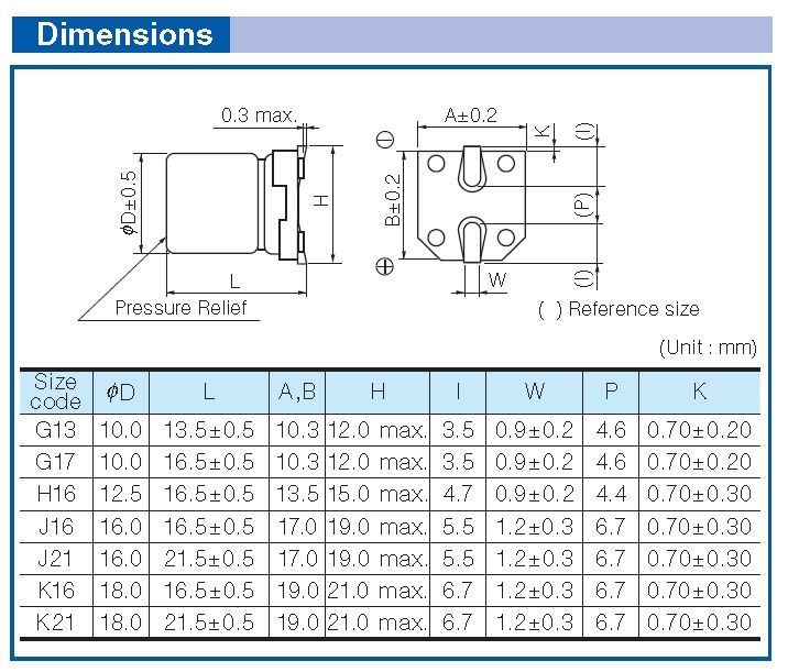 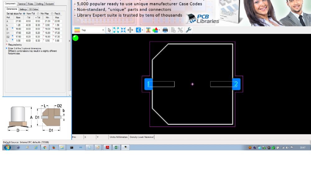 whats wrong am doing? please help
|
|
 |
|

|
|
|
|
|
Tom H
Admin Group 

Joined: 05 Jan 2012 Location: San Diego, CA Status: Offline Points: 6070 |
Post Options
Thanks(1)
Quote Reply
Posted: 12 Sep 2016 at 7:09am |
|
Do you see the blue dots in the dimensions? Only enter any 2 of 3 that you want and never enter all 3. You'll get bad results due to over calculation of tolerances. |
|
|
|
|
Sujith
Active User
Joined: 12 Sep 2016 Status: Offline Points: 22 |
Post Options
Thanks(1)
Quote Reply
Posted: 12 Sep 2016 at 8:43am |
|
Ahh..yes, I missed it.
It got worked now..  . .In the component data sheet by the mafr the pads values are : L=5.5, W=1.2+-0.3, P=6.7 . is this values are based on nominal or most or least? and the generated footprints measurement were : Most Nominal Least L=6.83 L=6.46 L=6.12 W=2.7 W=2.52 W=2.31 other dimensions like outline and courtyards also varies, i didt checked. here I got the width of the pads entirely wrong it seems? and its a bit confusing which footprint (n,m,l) to use , in the internet most people suggests to use nominal footprints. Actually what is the best practice to follow?
|
|
|
|
|
Tom H
Admin Group
Joined: 05 Jan 2012 Location: San Diego, CA Status: Offline Points: 6070 |
Post Options
Thanks(1)
Quote Reply
Posted: 12 Sep 2016 at 9:08am |
|
Most people use Nominal Density Level, which is a default setting. Maximum Density is used for space satellites. Least Density Level is used for RF design or extremely dense designs. |
|
|
|
|
Sujith
Active User
Joined: 12 Sep 2016 Status: Offline Points: 22 |
Post Options
Thanks(1)
Quote Reply
Posted: 12 Sep 2016 at 9:36pm |
|
Ok...thanks for the info.
but how to get the correct pad width? instead of 1.2 +-0.3 am getting 2.51
|
|
|
|
|
Tom H
Admin Group
Joined: 05 Jan 2012 Location: San Diego, CA Status: Offline Points: 6070 |
Post Options
Thanks(0)
Quote Reply
Posted: 13 Sep 2016 at 7:38am |
|
The solder joint goals in LE Lite are in the tab Terminal > Density Level > Toe, Heel and Side. You can control the entire solder joint by adjusting those values. |
|
|
|
|
Post Reply
|
|
| Tweet |
| Forum Jump | Forum Permissions You cannot post new topics in this forum You cannot reply to topics in this forum You cannot delete your posts in this forum You cannot edit your posts in this forum You cannot create polls in this forum You cannot vote in polls in this forum |


 Topic Options