

|
|
copper on one side of through hole |
Post Reply 
|
| Author | |
rtennill 
Active User 
Joined: 02 Aug 2016 Status: Offline Points: 23 |
 Post Options Post Options
") Thanks(0) Thanks(0)
 Quote Reply Quote Reply
 Topic: copper on one side of through hole Topic: copper on one side of through holePosted: 07 Oct 2016 at 5:57pm |
|
I am trying to match the recommended pattern for a Molex 513870530 surface mount mini-USB connector. It requires two slotted through holes with no copper on the top side and copper pads on the bottom layer.
I have created this pattern several times in FP Designer and it looks good until I try to reload the part either by reloading the FPX or switching to a different part and coming back. When it reloads the part, I end up with just the slotted holes and what looks like an anti-pad on the bottom instead of the copper ring it was showing when I saved it. I've tried plated and non-plated hole but with same results. I know I can put some copper on the top layer but I'd like to figure this out in case I come across a case where that's not an option. I've attached the drawing and images of my settings if someone has a few minutes to take a look. 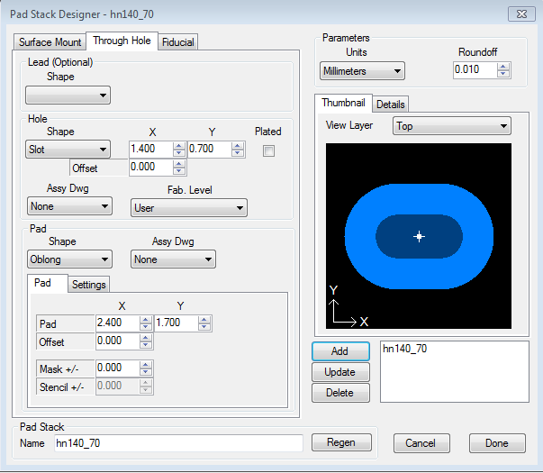 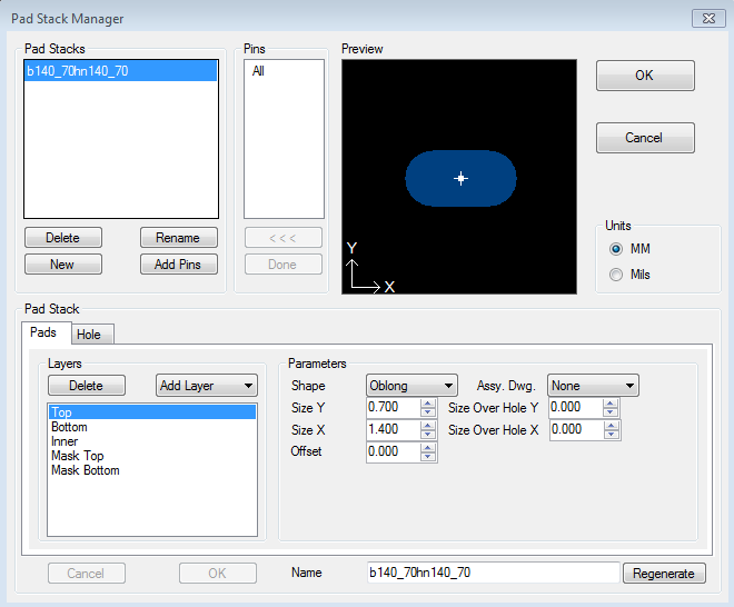 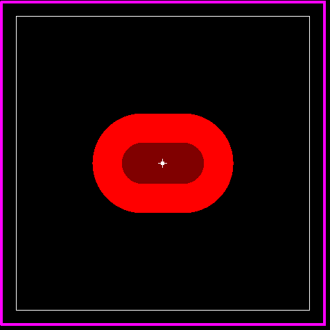 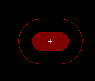 |
|
 |
|
|
|
|
Tom H
Admin Group 

Joined: 05 Jan 2012 Location: San Diego, CA Status: Offline Points: 5716 |
Post Options
Thanks(0)
Quote Reply
Posted: 08 Oct 2016 at 7:59am |
|
After you create the slotted hole in Pad Stack Designer and add it to the Pad Stack list, select the Done button and open Pad Stack Manager. Select the "Top Layer" and in the Parameters section change Size Over Hole Y & X to zero "0". Then select the OK button below the Layers window to regenerate the pad stack name. You might also want to change the Top Solder Mask "Size Over Hole Y & X" to zero "0". Select the OK button in the upper Right corner when you're finished. |
|
|
|
|
rtennill
Active User
Joined: 02 Aug 2016 Status: Offline Points: 23 |
Post Options
Thanks(0)
Quote Reply
Posted: 17 Oct 2016 at 11:11am |
|
Looks like it's just a display issue. I already had Size Over Hole X|Y set to 0. I went ahead and saved the part and regenerated our PADS library. The bottom pads show up when the part is placed.
|
|
|
|
|
Tom H
Admin Group
Joined: 05 Jan 2012 Location: San Diego, CA Status: Offline Points: 5716 |
Post Options
Thanks(0)
Quote Reply
Posted: 16 Nov 2016 at 1:02pm |
|
This display issue is resolved in the new V2017.02 - www.pcblibraries.com/downloads |
|
|
|
|
Post Reply
|
|
| Tweet |
| Forum Jump | Forum Permissions You cannot post new topics in this forum You cannot reply to topics in this forum You cannot delete your posts in this forum You cannot edit your posts in this forum You cannot create polls in this forum You cannot vote in polls in this forum |


 Topic Options