

|
|
SOD882D Package = Dual Flat with lead |
Post Reply 
|
| Author | |
MSM_KOPF 
Advanced User 
Joined: 02 Feb 2015 Status: Offline Points: 53 |
 Post Options Post Options
") Thanks(0) Thanks(0)
 Quote Reply Quote Reply
 Topic: SOD882D Package = Dual Flat with lead Topic: SOD882D Package = Dual Flat with leadPosted: 03 May 2019 at 6:13am |
|
We use a Nexperia ESD Diode PESD5V0F1BL with a package called SOD882 That is a typical DFN which Library Expert Pro creates as DIODFN98X58X50-2N Datasheet see Digikey or Nexperia Due to AOI requirements we must move to the PESD5V0F1BLD what Nexperia calls a DFN1006-2 (SOD882D) package This component will be soldered at the side too, hence optical inspection possible But what surface mount type shall i choose to create the footprint? It is not a Dual Flat No_lead DFN 2 Pin But it is also not realy a molded body BTW we often come across this No Lead limitation that prevents us from using the calculator as we have a lead version. would be nice to select Lead / No-Lead.
|
|
 |
|
|
|
|
Ian S
Advanced User
Joined: 21 Aug 2014 Status: Offline Points: 67 |
Post Options
Thanks(1)
Quote Reply
Posted: 03 May 2019 at 8:00am |
|
My suggestion would be to use 'DFN 2 Pin' and, after entering the component's dimensions, switch to the Footprint tab and enter the manufacturer's recommended dimensions from the datasheet.
|
|
|
|
|
Tom H
Admin Group 

Joined: 05 Jan 2012 Location: San Diego, CA Status: Offline Points: 5716 |
Post Options
Thanks(0)
Quote Reply
Posted: 03 May 2019 at 8:57am |
|
The Nexperia ESD Diode PESD5V0F1BL with a package called SOD882 is a 2-pin DFN package.
This is a standard component package and Library Expert creates a perfect 3D STEP model too. 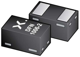 |
|
|
|
|
MSM_KOPF
Advanced User
Joined: 02 Feb 2015 Status: Offline Points: 53 |
Post Options
Thanks(0)
Quote Reply
Posted: 05 May 2019 at 10:39pm |
|
If i use the manufacturing recommended footprint, then there is no need to use library expert tool. But: Manufacture Nexperia recommends a width (W) of 0.7mm whereas Library expert uses only 0.53mm width pads. So i am asking gain, what would be the way to create a PESD5V0F1BLD DFN1006-2 (SOD882D) footprint with the library expert pro. both packages and footprints are a bit different.
|
|
|
|
|
Tom H
Admin Group
Joined: 05 Jan 2012 Location: San Diego, CA Status: Offline Points: 5716 |
Post Options
Thanks(0)
Quote Reply
Posted: 06 May 2019 at 7:15am |
|
Library Expert uses nominal values for Toe, Heel and Side solder joint goals + the fabrication and assembly tolerance + the component package and Lead Tolerances.
All of these dimensions are guidelines and not set in stone. They are not a standard, but they are for you to use as a base starting point for you to make the decision of what your actual solder joint goal values should be and what your manufacturing and package tolerances should be. All of these things affect the calculation of the resulting pad size. Library Expert is a tool that enables you to change any of the values to whatever you want, including the insertion of the mfr. recommended pattern. Library Expert allows you to see the Terminal Lead on the resulting pad so that you can make an educated judgement for the best soldering results. Library Expert auto-generates the drafting outlines for silkscreen Legend, Assembly, Courtyard Excess, Package Body and Terminal Lead and it adds the Pin 1 polarity marking and the proper reference designators. There is no land pattern calculator in the world that will magically calculate every mfr. recommended pattern and the mfr. will only provide the pad size and spacing and not all the other elements that go into a library part. |
|
|
|
|
Post Reply
|
|
| Tweet |
| Forum Jump | Forum Permissions You cannot post new topics in this forum You cannot reply to topics in this forum You cannot delete your posts in this forum You cannot edit your posts in this forum You cannot create polls in this forum You cannot vote in polls in this forum |


 Topic Options