

|
|
Transistor Outline (TO, DPAK) query |
Post Reply 
|
| Author | |
jameshead 
Expert User 

Joined: 20 Mar 2012 Location: Oxfordshire, UK Status: Offline Points: 576 |
 Post Options Post Options
") Thanks(0) Thanks(0)
 Quote Reply Quote Reply
 Topic: Transistor Outline (TO, DPAK) query Topic: Transistor Outline (TO, DPAK) queryPosted: 24 Jul 2012 at 2:49am |
|
Could you confirm that this view and calculation is okay for National Semiconductor part LM2595S?
The datasheet is here: http://www.ti.com/lit/ds/symlink/lm2595.pdf But there's a better drawing here: http://www.national.com/packaging/mkt/ts5b.pdf Entered dimensions were: 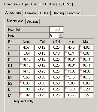 D1 and D were put in as the same value. E Min was put in as 13.85 mm based on using a +/- 0.25 mm tolerance which I used based on the main tolerance they'd used of +/- 0.25 else where on the drawing - not too disimilar to the +/- 0.2 mm tolerance suggested by Tom earlier for missing dimensions. I took L1 from the datasheet as 1.27 max and made a similar application of a +/- 0.25 mm tolerance, then worked out E1, E, and E2. E1 max = 1.27 + (8.64 + 0.25) = 10.16 mm E1 min = (1.27 - 0.5) + (8.64 - 0.25) = 9.16 mm E2 max = 1.27 + (5.08 + 0.5) = 6.85 mm E2 min = (1.27 - 0.5) + 5.08 = 5.85 mm L was given as 1.98 with no tolerance so again I put in a +/- 0.25 mm tolerance. L1 max = 1.27 mm L1 min = 1.27 - 0.5 = 0.77 mm Dimensions shown after entry were: 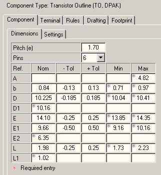 Footprint view is: 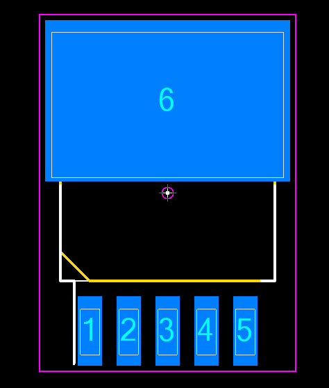 Normally I'd not be too bothered if I was just doing this footprint for myself but I am conciously aware that these may end up in FPX files used by others so just wanted some feedback on what's expected for these packages. |
|
 |
|
|
|
|
Tom H
Admin Group 

Joined: 05 Jan 2012 Location: San Diego, CA Status: Offline Points: 5716 |
Post Options
Thanks(1)
Quote Reply
Posted: 23 Oct 2012 at 8:27pm |
|
The mfr. does not provide the Maximum Thermal pad length (dimension "E2").
In that case, you should always Tweak the E2 dimension so that the Pad Length is at least equal to the mfr. recommended footprint (land pattern). The recommended footprint E2 dimension for one of the parts is - 10.41 mm - http://www.ti.com/lit/ds/symlink/lm2595.pdf So there are 2 different footprint patterns (2 different FPX files). If you personally want to make a singe pattern that will fit both parts then you need to use the largest E2 value of the 2 components. You can also use the "Footprint" tab and enter the mfr recommended footprint values to create that unique pattern. |
|
|
|
|
Post Reply
|
|
| Tweet |
| Forum Jump | Forum Permissions You cannot post new topics in this forum You cannot reply to topics in this forum You cannot delete your posts in this forum You cannot edit your posts in this forum You cannot create polls in this forum You cannot vote in polls in this forum |


 query")


 Topic Options