|
|
PQFN/PSON Footprint Name |
Post Reply 
|
| Author | |
JZsori 
Advanced User 
Joined: 01 Mar 2012 Status: Offline Points: 65 |
 Post Options Post Options
") Thanks(0) Thanks(0)
 Quote Reply Quote Reply
 Topic: PQFN/PSON Footprint Name Topic: PQFN/PSON Footprint NamePosted: 01 Jun 2012 at 7:05pm |
|
There are multiple instances with the same name and description (PSON50P400X400X80-14, for example) but one has rectangular pads and the other has D-Shape pads. There should be some way to differentiate.
|
|
 |
|
|
|
|
Tom H
Admin Group 

Joined: 05 Jan 2012 Location: San Diego, CA Status: Offline Points: 5716 |
Post Options
Thanks(0)
Quote Reply
Posted: 22 Oct 2012 at 10:39am |
|
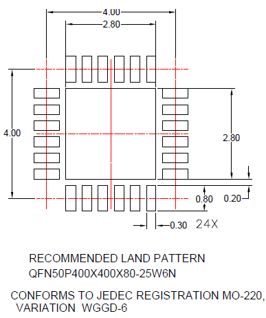
The Component Lead Shape and the resulting Pad Shape have nothing to do with the footprint pattern name. Here is a component manufacturer that produces QFN packages with D-shape Package Leads -
Here is their recommended footprint with Rectangular footprint pads. Also notice that the Component Thermal Tab has a Chamfer Corner by Pin 1 and rounded corners on the others, but the manufacturer recommends a solid square with no chamfer or rounded corners. So it's really a "User Option". Also note that the manufacturer is calling the footprint a "Land Pattern" and they are using the IPC-7351 Land Pattern Naming Convention with the JEDEC variation in the Land Pattern Name (W6) to discriminate the Thermal Pad size. |
|
|
|
|
Sanand
New User 

Joined: 27 Oct 2012 Location: California Status: Offline Points: 1 |
Post Options
Thanks(0)
Quote Reply
Posted: 27 Oct 2012 at 2:01am |
|
Hi,
I am new user for this site. I have some questions regarding the land pattern and wonder if this forum is suit for it. Do you know of any minimum clearance along the edge of PCB or memory module must be? Is it 0.050" to be minimum or 0.150"? And minimum gap between to components footprint or between two terminals of passive 0201? Thanks |
|
|
|
|
Tom H
Admin Group
Joined: 05 Jan 2012 Location: San Diego, CA Status: Offline Points: 5716 |
Post Options
Thanks(0)
Quote Reply
Posted: 27 Oct 2012 at 8:02am |
|
The minimum board edge to any feature - component, via, trace, copper pour is 40 mils (1.0 mm).
The minimum SMT component to component body or component pad to component pad gap is 10 mil (0.25 mm) for different components. The minumum pad to pad gap on the same component is 6 mils (0.15 mm). The minimum pad to thermal pad gap on the same component is 8 mils (0.20 mm). You can also get more information by reading my blog here - Copy/Paste the entire Blog into a Word document or print it out to PDF. We don't know how long Mentor Graphics will keep it available. |
|
|
|
|
rdl86626
Advanced User

Joined: 20 Jul 2012 Location: Hollister, CA Status: Offline Points: 83 |
Post Options
Thanks(0)
Quote Reply
Posted: 29 Oct 2012 at 8:35am |
|
Tom, I was reading the form where you stated “The minimum board edge to any feature - component, via, trace, copper pour is 40 mils (1.0 mm)”. I have a hard time with IPC spec’s and where to find out things like that. I have been using .040 for planes and .020 for traces. What spec are these things in?
I don't mean to sound stupid,
Dumb Rick |
|
|
|
|
Tom H
Admin Group
Joined: 05 Jan 2012 Location: San Diego, CA Status: Offline Points: 5716 |
Post Options
Thanks(0)
Quote Reply
Posted: 29 Oct 2012 at 8:55am |
|
I don't get all of the rules from IPC, but they do document a lot of DFM stuff in the IPC-2221 and IPC-2222.
I use fabrication shops and common sense most of the time. Example: I went to Google and typed "DFM Guidelines" and I found this PDF file - http://irtfweb.ifa.hawaii.edu/~ao/Electronic/Peter_dump/Electronics/System/Text/PCBCADGuidelines.pdf This document produced in Hawaii surveyed several California Fabrication shops -
There are comparisons between manufacturers. You say to pull your planes back 40 mils but traces 20 mils. To me this means that you have traces without a reference plane below them. I wouldn't do that. The main reasons why features need to be pulled back from the board edge is the answer to your question. Is it because the fabrication shop is V-scoring or using a router. When breaking up the panel into individual boards, V-Scoreing can leave rough edges that need to be panelerized plus the process requires recessed features as not to damage them. Does your panel need to remain intact for assembly? If so, there will be breakaway rat-bite holes in the router process. |
|
|
|
|
rdl86626
Advanced User
Joined: 20 Jul 2012 Location: Hollister, CA Status: Offline Points: 83 |
Post Options
Thanks(0)
Quote Reply
Posted: 29 Oct 2012 at 9:07am |
|
Thanks Tom,
Thank you very much and I see your point. We have boards that are ridgid flex with analog /digial mixed. I have 1 or 2 traces that break that rule, which I do break if I have to, like you say common sense is the best rule. Thanks again. not so dumb Rick |
|
|
|
|
Post Reply
|
|
| Tweet |
| Forum Jump | Forum Permissions You cannot post new topics in this forum You cannot reply to topics in this forum You cannot delete your posts in this forum You cannot edit your posts in this forum You cannot create polls in this forum You cannot vote in polls in this forum |


 Topic Options