

|
|
Odd Looking Footprint for Chip Array |
Post Reply 
|
| Author | |
LaserAlex 
Active User 

Joined: 06 Jun 2012 Location: Seattle, WA Status: Offline Points: 27 |
 Post Options Post Options
") Thanks(0) Thanks(0)
 Quote Reply Quote Reply
 Topic: Odd Looking Footprint for Chip Array Topic: Odd Looking Footprint for Chip ArrayPosted: 25 Aug 2012 at 2:03am |
|
I was trying to create a footprint for a small (quad 0201) Panasonic chip array resistor. The footprint created by PCB Footprint Expert has really skinny lands, when compared to both the manufacturer's recommended footprints and the Mentor IPC footprint calculator I got with my copy of the IPC standard.
Is this a bug, or has the standard changed? Thanks! 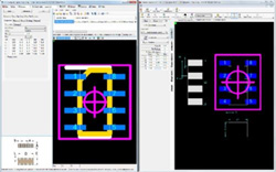 |
|
 |
|

|
|
|
|
|
Tom H
Admin Group 

Joined: 05 Jan 2012 Location: San Diego, CA Status: Offline Points: 6088 |
Post Options
Thanks(0)
Quote Reply
Posted: 25 Aug 2012 at 8:51am |
|
With 0201 microminiature components, less solder is sometimes best and according to the IPC-7351 mathematical model that's true.
However, if the component manufacturer did their due diligence and tested their recommended pattern and it passed all stress tests then I would consider using it. That is why we built into the new PCB Footprint Expert the ability to enter the component manufacturer recommended pattern dimensions. Every component family has a "Footprint" tab. After you insert all the component dimensions and select "OK" to calculate the IPC pattern, select the "Footprint" tab to compare the IPC pattern with the manufacturer's pattern dimensions. If they're way off, select the "Use Manufacturer's Recommended Dimensions" button and enter the pad length, width and separation dimensions and build that pattern. The IPC rules for Courtyard spacing will be auto-calculated and the silkscreen will be auto-trimmed to follow your silkscreen to pad rule. 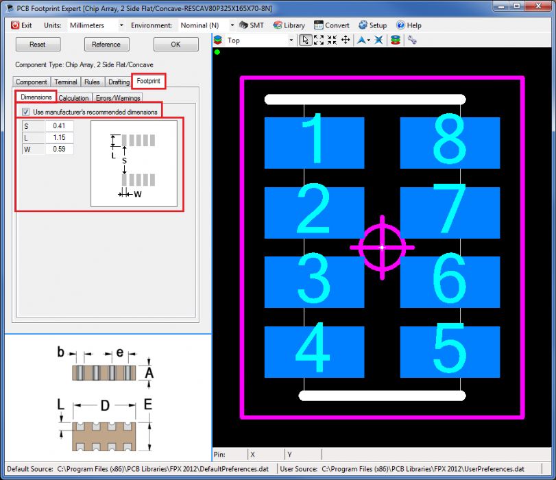 |
|
|
|
|
LaserAlex
Active User
Joined: 06 Jun 2012 Location: Seattle, WA Status: Offline Points: 27 |
Post Options
Thanks(0)
Quote Reply
Posted: 28 Aug 2012 at 12:41pm |
|
Thanks, Tom.
I'm OK with the general idea of entering the manufacturer's preferred footprint. However, it doesn't explain why PCB Footprint Expert gives a different recommended footprint than LP Wizard. If they are both using the same version of the IPC standard for their calculations, they should both produce identical land patterns. The fact that they don't seems like a possible bug to at least look in to.
In the mean time, I have created a footprint according to the manufacturer's instructions, I just want to make sure this doesn't cause a problem for any other users in the future. Regards, -Alex |
|
|
|
|
Tom H
Admin Group
Joined: 05 Jan 2012 Location: San Diego, CA Status: Offline Points: 6088 |
Post Options
Thanks(0)
Quote Reply
Posted: 28 Aug 2012 at 12:47pm |
|
The PCB Footprint Expert is a brand new tool that was written from scratch and during the process we discovered some mistakes we made with LP Wizard.
Also, the new program uses a higher resolution of 0.01 mm snap grid round-off while LP Wizard uses a 0.05 mm round-off. If there are differences, they should only be 1 or 2 mils. |
|
|
|
|
Jeff.M
Admin Group

Joined: 16 May 2012 Location: San Diego Status: Offline Points: 501 |
Post Options
Thanks(0)
Quote Reply
Posted: 28 Aug 2012 at 12:48pm |
|
Can you send us the datasheet (or link) for the part you're creating so we can check it?
|
|
|
|
|
LaserAlex
Active User
Joined: 06 Jun 2012 Location: Seattle, WA Status: Offline Points: 27 |
Post Options
Thanks(0)
Quote Reply
Posted: 28 Aug 2012 at 1:48pm |
|
Sure, here's a top-level link:
The catalog with dimensions is here: and the recommended footprint is here: If you look at the image in my first post, you'll see that Footprint Expert makes pads that are half as wide and twice as long as the recommended land pattern. The LP Wizard comes up with something pretty close to the manufacturer's recommendation. |
|
|
|
|
Tom H
Admin Group
Joined: 05 Jan 2012 Location: San Diego, CA Status: Offline Points: 6088 |
Post Options
Thanks(0)
Quote Reply
Posted: 29 Aug 2012 at 8:23am |
|
To summarize, the significant differences are: 1. In the Toe Goal…the manufacturer is ignoring the IPC toe 2. In the Heel Goal…the manufacturer is ignoring the IPC heel 3. LPW has a smaller IPC toe than FPX (bug in LPW) 4. LPW has different place and size rounds. 0.05 mm for LPW and 0.01 mm for FPX 5. Finally, LPW has a minimum pad-to-pad spacing rule of 0.20 mm so it’s heel is being trimmed more than FPX which has a minimum pad to pad of 0.15 mm. |
|
|
|
|
Post Reply
|
|
| Tweet |
| Forum Jump | Forum Permissions You cannot post new topics in this forum You cannot reply to topics in this forum You cannot delete your posts in this forum You cannot edit your posts in this forum You cannot create polls in this forum You cannot vote in polls in this forum |


 Topic Options