|
|
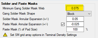
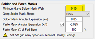
Minimum Gang Solder Mask Web |
Post Reply 
|
| Author | |
yvoren1 
New User 

Joined: 07 Jun 2013 Status: Offline Points: 17 |
 Post Options Post Options
") Thanks(1) Thanks(1)
 Quote Reply Quote Reply
 Topic: Minimum Gang Solder Mask Web Topic: Minimum Gang Solder Mask WebPosted: 19 Dec 2023 at 1:17pm |
|
Hi, I’d like to understand how work Minimum Gang Solder
Mask Web in SMD Pad Stack Rules I have these specifications in Component Data
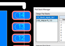
If I use 0.10 mm for the Minimum Gang Solder web mask, I get a 0.83 x 0.40 mm mask, so the web mask = 0.10 mm that is correct
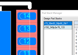
If I use 0.10 mm for the Minimum Gang Solder web mask, I get a 0.83 x 0.50 mm mask, hence the web mask. I don't understand why the mask becomes 0.40 mm to 0.50 mm. I expected the mask to stay at 0.40 mm for a 0.10 mm web
|
|
 |
|

|
|
|
|
|
Tom H
Admin Group 

Joined: 05 Jan 2012 Location: San Diego, CA Status: Offline Points: 6088 |
Post Options
Thanks(0)
Quote Reply
Posted: 19 Dec 2023 at 4:35pm |
|
Are you wondering why the
solder mask excess isn’t limited to prevent a sliver instead of increased to
fill the sliver?
|
|
|
|
|
yvoren1
New User
Joined: 07 Jun 2013 Status: Offline Points: 17 |
Post Options
Thanks(0)
Quote Reply
Posted: 20 Dec 2023 at 6:43am |
|
Yes, that’s what I would like to know!
|
|
|
|
|
Tom H
Admin Group
Joined: 05 Jan 2012 Location: San Diego, CA Status: Offline Points: 6088 |
Post Options
Thanks(0)
Quote Reply
Posted: 20 Dec 2023 at 9:57am |
|
First, setting the solder mask web to 0.10 is overkill.
Fabrication shops can easily produce a 0.07 solder mask sliver. Where the Fabrication industry needs is a 0.05 mm solder mask swell and a 0.05 solder mask web. This will ensure a solder mask sliver between every SMD pad stack and eliminate Gang Masking of entire rows of pads. Ask your fabrication shop how accurate is their solder mask application process. |
|
|
|
|
yvoren1
New User
Joined: 07 Jun 2013 Status: Offline Points: 17 |
Post Options
Thanks(1)
Quote Reply
Posted: 20 Dec 2023 at 10:04am |
|
OK ,
Some of my fab shop don't want to go under 0.1mm , but now i know how far i can go Thank you Tom!
|
|
|
|
|
Tom H
Admin Group
Joined: 05 Jan 2012 Location: San Diego, CA Status: Offline Points: 6088 |
Post Options
Thanks(0)
Quote Reply
Posted: 20 Dec 2023 at 10:12am |
|
There is something you need to know.
If your fabrication shop requires a 0.10 mm solder mask sliver, if you don't Gang Mask the row of pads in your PCB library, your fabrication shop will run a check on your Gerber data to find every pad that has a sliver less than 0.10 mm and they will gang mask the row of pads without even asking you. So either you provide the correct data or they will correct your data. |
|
|
|
|
bab27
New User
Joined: 01 Sep 2024 Status: Offline Points: 13 |
Post Options
Thanks(1)
Quote Reply
Posted: 03 Sep 2024 at 5:58am |
|
I'm looking for an IPC for these kinds of specification.
IPC-7352 Page 34, there is an example with 0.50 mm Pitch SOP with 0.05 mm Solder Mask from copper and 0.075 mm from Solder Mask to Legend (silkscreen). Do you know if there is more information according to the fabrication level, A, B or C about that? |
|
|
|
|
Tom H
Admin Group
Joined: 05 Jan 2012 Location: San Diego, CA Status: Offline Points: 6088 |
Post Options
Thanks(1)
Quote Reply
Posted: 03 Sep 2024 at 8:15am |
|
I provided IPC-7352 with the silkscreen and solder mask illustration on page 34. As PCB designers we all create prototype boards that require silkscreen for small batches. We recommend a silkscreen line width between 0.12 mm minimum, 0.15 mm nominal and 0.20 mm maximum. IPC has no rules or guidelines on solder mask. The current range for solder mask annular ring in the electronics industry (from component manufacturers recommendations) is between 0.05 mm minimum, 0.07 mm nominal and 0.10 mm maximum. The gap between the silkscreen and solder mask would be the tolerance of the application of both, which is 0.07 total. You don't want any silkscreen encroaching in the solder mask removal area. If there is silkscreen in the solder mask removal area, the fabrication shop will automatically trim it off for you. |
|
|
|
|
bab27
New User
Joined: 01 Sep 2024 Status: Offline Points: 13 |
Post Options
Thanks(1)
Quote Reply
Posted: 11 Sep 2024 at 7:40am |
|
Thank you very much for your reply.
|
|
|
|
|
Post Reply
|
|
| Tweet |
| Forum Jump | Forum Permissions You cannot post new topics in this forum You cannot reply to topics in this forum You cannot delete your posts in this forum You cannot edit your posts in this forum You cannot create polls in this forum You cannot vote in polls in this forum |


 Topic Options