

|
|
Bug with 3D output of SOFL |
Post Reply 
|
| Author | |
JeffreyJ 
New User 

Joined: 03 Oct 2012 Status: Offline Points: 3 |
 Post Options Post Options
") Thanks(0) Thanks(0)
 Quote Reply Quote Reply
 Topic: Bug with 3D output of SOFL Topic: Bug with 3D output of SOFLPosted: 24 May 2017 at 4:29pm |
|
Hi, I create a transformer using transistor footprint SOFL since it used the same package. But the XFMR has a slightly rotated pinout which I was able to change for the land pattern. But when I generated the 3d Step file, the pin 1 marking didn't follow along and is incorrect in the step file.
Please see images below. 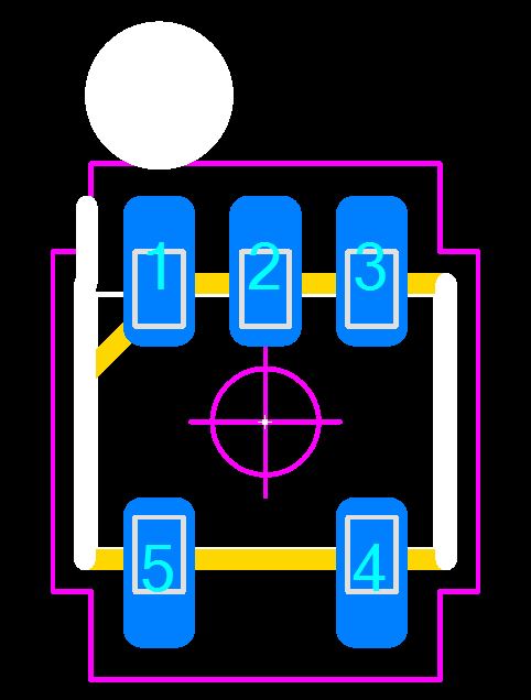 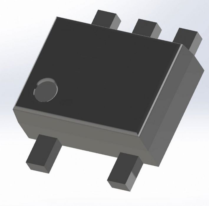 If you have any questions, please feel free to contact me. Jeffrey Jenkins
|
|
 |
|

|
|
|
|
|
Tom H
Admin Group 

Joined: 05 Jan 2012 Location: San Diego, CA Status: Offline Points: 6088 |
Post Options
Thanks(0)
Quote Reply
Posted: 24 May 2017 at 4:33pm |
|
Do you want us to add "Transformer" to the component selection? Do you want us to add "Pin Rename" to the SOFL component family? You can move the part to FP Designer and do whatever you want. But you can use the Calculator to produce a high quality 3D STEP. |
|
|
|
|
JeffreyJ
New User
Joined: 03 Oct 2012 Status: Offline Points: 3 |
Post Options
Thanks(0)
Quote Reply
Posted: 24 May 2017 at 5:03pm |
|
Hi Tom,
I don't really need any of those. What the issue is the pin 1 marking on the Step file output didn't follow the pin 1 on the part when it was mirrored and rotated inside of Library Expert (version 2017.13). The footprint for xPCB cell was fine, but the STEP file output was incorrect. This appears to be a bug.
|
|
|
|
|
Tom H
Admin Group
Joined: 05 Jan 2012 Location: San Diego, CA Status: Offline Points: 6088 |
Post Options
Thanks(0)
Quote Reply
Posted: 24 May 2017 at 5:08pm |
|
OK, it's a STEP file bug and we will direct that to the correct programmer. Thanks! |
|
|
|
|
Tom H
Admin Group
Joined: 05 Jan 2012 Location: San Diego, CA Status: Offline Points: 6088 |
Post Options
Thanks(0)
Quote Reply
Posted: 25 May 2017 at 3:40pm |
|
This issue is now fixed in V2017.14 pre-release - www.pcblibraries.com/downloads |
|
|
|
|
Post Reply
|
|
| Tweet |
| Forum Jump | Forum Permissions You cannot post new topics in this forum You cannot reply to topics in this forum You cannot delete your posts in this forum You cannot edit your posts in this forum You cannot create polls in this forum You cannot vote in polls in this forum |


 Topic Options