|
|
Footprint for Chip Tantalum Capacitor With Nib |
Post Reply 
|
Page 12> |
| Author | |
lsday 
Active User 
Joined: 15 Dec 2014 Status: Offline Points: 24 |
 Post Options Post Options
") Thanks(0) Thanks(0)
 Quote Reply Quote Reply
 Topic: Footprint for Chip Tantalum Capacitor With Nib Topic: Footprint for Chip Tantalum Capacitor With NibPosted: 15 Dec 2014 at 8:14am |
|
Why haven't you come up with footprints for the capacitors with nibs? These type capacitors always seem to be a problem to calculate footprints for?
|
|
 |
|

|
|
|
|
|
Tom H
Admin Group 

Joined: 05 Jan 2012 Location: San Diego, CA Status: Offline Points: 6070 |
Post Options
Thanks(0)
Quote Reply
Posted: 15 Dec 2014 at 9:06am |
|
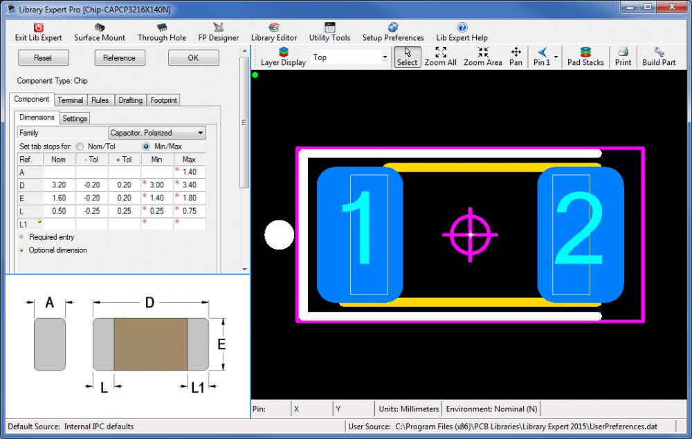
We have Capacitors with Nibs for a long time. They are "Chip, Polarized Capacitors" and the 3D STEP model looks perfect from Library Expert. |
|
|
|
|
lsday
Active User
Joined: 15 Dec 2014 Status: Offline Points: 24 |
Post Options
Thanks(0)
Quote Reply
Posted: 15 Dec 2014 at 9:23am |
|
I am not interested in a 3D model. I want to be able to calculate a landpattern from the viewer and there is no choice for that. I am am new to your calculator and it is the free one.
|
|
|
|
|
Tom H
Admin Group
Joined: 05 Jan 2012 Location: San Diego, CA Status: Offline Points: 6070 |
Post Options
Thanks(0)
Quote Reply
Posted: 15 Dec 2014 at 9:28am |
|
The choice is "Chip, Capacitor, Polarized"
|
|
|
|
|
lsday
Active User
Joined: 15 Dec 2014 Status: Offline Points: 24 |
Post Options
Thanks(0)
Quote Reply
Posted: 15 Dec 2014 at 9:35am |
|
I see it now. I spoke too soon without actually looking at the viewer properly.
|
|
|
|
|
carkifelek
New User 
Joined: 05 Jan 2015 Status: Offline Points: 1 |
Post Options
Thanks(0)
Quote Reply
Posted: 05 Jan 2015 at 3:47pm |
|
Tom, It actually is a little confusing. I actually had to spend some time getting the correct footprint for these polar capacitors. If the name could simply be changed to polarized capacitors, it might actually save some time for other people who’ll be having this issue in the future. I’m not saying it’s an issue per se but it might just make it easier for people to search for these pads. |
|
|
|
|
Tom H
Admin Group
Joined: 05 Jan 2012 Location: San Diego, CA Status: Offline Points: 6070 |
Post Options
Thanks(0)
Quote Reply
Posted: 05 Jan 2015 at 6:10pm |
|
We'll be releasing a new document this week that clearly defines every component family with 3D model pictures, land patterns, pin assignments, silkscreen, zero component orientation, recommended pad shape, component lead terminals superimposed with pad (graphic on a mechanical layer) in the CAD footprint and solder joint goal tables for each lead style. |
|
|
|
|
Louis_Guerin
Active User

Joined: 29 Jan 2013 Location: Quebec Status: Offline Points: 24 |
Post Options
Thanks(0)
Quote Reply
Posted: 16 Oct 2015 at 8:20am |
|
Hi Tom, I'm a bit confused when I look at the table from Vishay; http://www.vishay.com/docs/40006/594d.pdf I try to build one having the case C but some value given are either max or ref. Also does dimension J is important in this case? |
|
|
|
|
Tom H
Admin Group
Joined: 05 Jan 2012 Location: San Diego, CA Status: Offline Points: 6070 |
Post Options
Thanks(0)
Quote Reply
Posted: 16 Oct 2015 at 8:26am |
|
Use these dimensions: D = body Length W - Body Width A = Terminal Width H = Height Do not use the L or J dimensions. The NIB sticks up in the air and solder goes under it. Use the Polarized Capacitor component family. |
|
|
|
|
Louis_Guerin
Active User
Joined: 29 Jan 2013 Location: Quebec Status: Offline Points: 24 |
Post Options
Thanks(0)
Quote Reply
Posted: 16 Oct 2015 at 8:40am |
|
Hi Tom,
D does not have a min or max or tolerance, in this case do I put 6mm on both min and max? Also does the courtyard will be enough for the max component lenght of 7.1mm which IMHO should not be centered?
|
|
|
|
|
Post Reply
|
Page 12> |
| Tweet |
| Forum Jump | Forum Permissions You cannot post new topics in this forum You cannot reply to topics in this forum You cannot delete your posts in this forum You cannot edit your posts in this forum You cannot create polls in this forum You cannot vote in polls in this forum |


 Topic Options