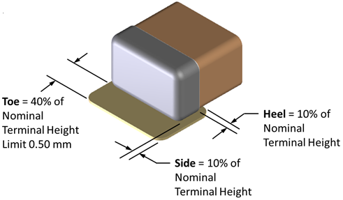
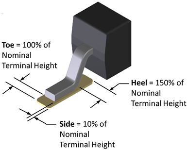
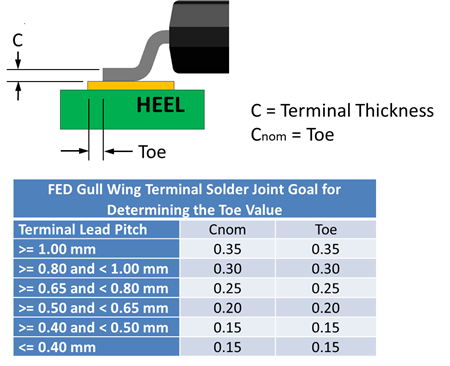
The IPC-7351B and IPC-7352 uses package and terminal lead tolerances in their mathematical model to calculate pad stacks for land patterns of standard component families. Component manufacturers provide nominal package dimensions and +/- tolerances. The problem arises as these package tolerances vary from one component manufacturer to another, leading to multiple footprint variations for the same component family. Using package tolerances for footprint calculation produces many different footprints for the same component family from different vendors.
Why is this a problem? Most Printed Circuit Board assemblers have multiple approved vendors for the same component package, as single sourcing components is uncommon. Companies often avoid using components with only one available vendor unless the component is critical to the product functionality.
For example, an 0603 chip component package may have tolerances ranging from 0.05 mm to 0.25 mm, resulting in multiple unique 0603 footprints across different vendors. These 0603 resistor component vendors have different package tolerances – Vishay, Panasonic, AVX, Stackpole, Yageo, ROHM, KOA, Samsung, Susumu, Bourns, Taiyo Yuden, TT Electronics, NIC, Ohmite, TE Connectivity, etc. Consequently, applying the IPC-7351 calculations will produce a unique footprint for each vendor, which is undesirable for standardization. The goal for a CAD librarian is to create a single footprint to accommodate all vendors for the same component package.
There are two solutions to address this issue:
- Use the same package tolerances for all vendors, regardless of the datasheet specification.
- Use nominal package dimensions and hard code solder joint goals for Toe, Heel, and Side.
The first approach uses the IPC-7351 mathematical model for footprint calculation. The second approach relies on nominal package dimensions with highly reliable solder joint goals, avoiding the variability caused by package and terminal lead tolerances.
Reasons to favor nominal dimensions for land pattern calculations:
- Improved Manufacturing Precision: Modern machines and manufacturing processes for electronic components and PCBs are highly accurate, producing components and assemblies that closely adhere to nominal dimensions.
- Industry Standards: Most component manufacturers recommend solder patterns in their datasheets are based on Nominal package dimensions with pre-defined solder joint goals. Few use the IPC-7351 mathematical model, which incorporates manufacturing tolerances.
- Tolerance Variability: Component package tolerances differ widely between manufacturers, complicating footprint standardization. This raises questions about the necessity and accuracy of these tolerances. Are they practical and realistic?
- Obsolete Complexity: The IPC-7351 mathematical model, originally created in the 1980s, is overly complex for today’s technology. IPC uses the Maximum Material Condition for calculations, which often results in unnecessarily large pad stacks.
- European Standards Alignment: The European standards organization FED (www.fed.de) advocates using Nominal package dimensions for land pattern calculations. Rainer Taube, a member of the FED board of directors and founder of Taube Electronic in Berlin, published FED Vol 18 “The New Proportional Land Pattern Dimensioning Concept” in 2018 which calls for the use of Nominal package dimensions and terminal height percentages for pad stack calculations.
Here is Rainer Taube’s mathematical model for land pattern calculation for two popular standard component packages. This closely resembles guidelines in the IPC J-STD-001 Standard. Although this land pattern solution also still creates duplication due to various terminal lead heights, a lot is simplified by utilizing the average terminal lead height for each component chip size package and each pin pitch for gullwing packages. The solder joint goals for Toe, Heel and Side can be hard coded. This concept will minimize duplication of footprints in CAD libraries.
Additional Considerations
In 1990, the EIA standards organization created the PDP-100 publication, which documented chip package case codes Length and Width dimensions, but not package height. If chip component manufacturers used the same height for each package case code, it would further reduce footprint duplication. For instance, 0603 chip capacitors are normally thicker (average 0.90 mm) than 0603 chip resistors (average 0.50 mm). It would be acceptable to define an average package height for each component family and case code. This would create a different footprint for each component family for Capacitor, Resistor, Inductor, Diode, etc. because they all have different 3D STEP models anyway.
These pad stack calculation percentages of terminal height have a tolerance of +/-5% and are reasonable for ensuring simple, clean, consistent, and reliable libraries.
EXAMPLE 1 - Rectangular End Cap (Chip) Leads:
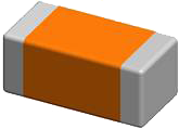
Common Chip Component Packages have different 3D STEP models:
|
Chip Capacitor
|
Chip Resistor
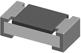
|
Chip Inductor
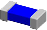
|
|
Polarized Chip Capacitor
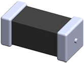
|
Chip Diode
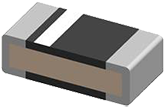
|
Chip LED
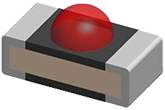
|
EIA Standard Chip Component Package Sizes with no Standard Height
reference
|
Table of Chip
Package Size Codes and Dimensions
|
|
EIA (inch) Name
|
Inch Dimensions
|
IEC (metric) Name
|
Metric Dimensions
|
|
01005
|
0.0157 in × 0.0079 in
|
0402
|
0.4 mm × 0.2 mm
|
|
0201
|
0.024 in × 0.012 in
|
0603
|
0.6 mm × 0.3 mm
|
|
0402
|
0.039 in × 0.020 in
|
1005
|
1.0 mm × 0.5 mm
|
|
0603
|
0.063 in × 0.031 in
|
1608
|
1.6 mm × 0.8 mm
|
|
0805
|
0.079 in × 0.049 in
|
2012
|
2.0 mm × 1.25 mm
|
|
1008
|
0.098 in × 0.079 in
|
2520
|
2.5 mm × 2.0 mm
|
|
1206
|
0.126 in × 0.063 in
|
3216
|
3.2 mm × 1.6 mm
|
|
1210
|
0.126 in × 0.098 in
|
3225
|
3.2 mm × 2.5 mm
|
|
1806
|
0.177 in × 0.063 in
|
4516
|
4.5 mm × 1.6 mm
|
|
1812
|
0.18 in × 0.13 in
|
4532
|
4.5 mm × 3.2 mm
|
|
2010
|
0.197 in × 0.098 in
|
5025
|
5.0 mm × 2.5 mm
|
|
2512
|
0.25 in × 0.13 in
|
6332
|
6.4 mm × 3.2 mm
|
|
2920
|
0.29 in × 0.20 in
|
7451
|
7.4 mm × 5.1 mm
|
EXAMPLE 2 - Gullwing Leads:
PCB Libraries, Inc. added the Nominal Calculation Mode to Footprint Expert V25.02 as an alternative land pattern calculator in January 2025. Users can switch back and forth between IPC-7352 and the New Proportional Land Dimensioning Concept.
Create IPC or FED compliant footprints using package dimensions and your personal Options for pad stack rules, drafting outlines and solder joint goals.
Welcome to the future of PCB design with the PCB Footprint Expert software - it is precision, speed, and innovation at your fingertips. Get the ultimate solution for creating precise, effortless, error-free PCB footprint solder patterns! Register on the PCB Libraries website and request your free evaluation license and web-based demo today!
Message from Rainer Thuringer, FED-Chairman
 In addition to reliable components and circuit boards, reliable electronics require equally reliable production. Following assembly with a low placement tolerance, a flawless soldering process of the components is particularly important. This in turn requires that the pad stacks on the circuit board match the component terminals exactly. In addition to reliable components and circuit boards, reliable electronics require equally reliable production. Following assembly with a low placement tolerance, a flawless soldering process of the components is particularly important. This in turn requires that the pad stacks on the circuit board match the component terminals exactly.
In the early days of SMD soldering technology it was assumed that for a reliable solder connection the soldering surfaces on the PCB should be significantly larger than the component terminals themselves. This is still reflected today in the applicable standards of IPC-7351B and IEC 61191-2. Although repeatedly revised and adopted to the ever-finer structures, the currently defined specifications and calculation methods for creating the soldering surfaces fit less and less to the constantly changing component terminals, especially the smaller they become, above all because constant absolute values are specified for the protrusions.
For modern reflow soldering processes, these are outdated rules and measures, as practice has shown. Soldering surfaces that protrude too far generate lateral tensile forces, which in extreme cases can lead to the dreaded tombstoning (tombstone effect) in assemblies with chip components, for example, or solder bridges in multi terminal components. So, too much solder and area can have negative effects during the soldering process. In addition, any unnecessary use of space is a considerable disadvantage, especially for the densely populated assemblies with a high concentration density.
The constantly expanding, almost incalculable variety of component terminal shapes, sizes and grid dimensions requires an adaptive dimensioning of the corresponding soldering surfaces for optimum solder joints.
This is where the New Proportional Land Dimensioning Concept comes in. It enables the calculation of the suitable land on the circuit board in proportion to the size of the component terminal, considering the physical properties of the soldering process: wetting, capillary action and force transmission. In their interaction, however, they cause the solder meniscus and coverings specified in the applicable standards under reliability aspects without unnecessarily or negatively affecting too large pad areas.
The starting point for the proportional concept is the requirements at the solder joints as described in J-STD-001 and IEC 61191–2 on the one hand and a new specified simplified classification of components, according to their terminal types on the other.
While the IEC land pattern standards as well as the IPC–7351B differentiate the components according to package families, the proportional concept is based on a two-stage classification according to terminal types.
The advantages of the New Proportional Land Dimensioning Concept are: - Easily scalable
- Trouble-free adaptation also for future components
- Risk, minimization (e.g. bridging and paste printing, best adapted paste volumes)
- Higher reliability of the solder joints (error-reduced assembly process)
- Proportional land pattern leads to more space for the PCB layout routing process
The initiator and inventor of the Proportional Concept, Reiner Taube, as entrepreneur and owner of TAUBE ELECTRONIC GmbH, a high-tech assembly manufacturer, recognized the necessity of a new Pad dimensioning concept based on his own experience years ago. The road and process to today's concept was long and rocky. He began with the intention of modifying the current IPC standard accordingly. In particular, the difficulty of converting major American DoD companies has prolonged the process and to date has not enabled a new IPC standard. At numerous meetings with Tom Hausherr, owner of PCB Libraries, Inc. the IPC-FED reference calculator emerged from hours of discussions about the correct footprint design, and its calculation from the IPC-7351B land pattern calculator – an Excel based calculator program, which allows the calculator according to the IPC-7351B algorithms as well as according to the new proportional concept.
This provides a tool that the FED makes available to its members for download. The Library of Knowledge, Volume 18, first explains the previous IPC land pattern concept and then introduces the New Proportional Land Dimensioning Concept and the IPC-FED reference calculator and explains its use.
Additionally, the FED verification project which was launched in 2016 to ensure that the land areas calculated with the proportional concept result in reliable solder joints according to the requirements of J-STD-001and IPC-A-610. In this project a test board was designed which contains land patterns according to IPC-7351B Nominal Density Level for all component types as well as land pattern calculated according to the Proportional Concept. For the evaluation of reliability, several circuit boards were assembled and soldered in two production facilities, and then inspected and approved by an independent expert according to the acceptance criteria of the IPC-A-610.
On behalf of the FED, I would like to express my sincere thanks to Rainer Taube for this valuable work and for his free time which he has made available and continues to make available to the FED and its members free of charge. Rainer Taube has been a member of the FED since it's foundation and stands by its side in word indeed without interruption ever since, currently as board member for the directives and standards division and as Master Trainer for the IPC-A-610 and conveyor of the IEC WG12 in the TC91 working group, where a new standard for dimensioning and land pattern on circuit boards is currently being developed, including the New Proportional Land Dimensioning Concept.
Purchase the FED Volume 18 publication here: |


 Post Options
 Thanks(0)
 Quote
Quote  Reply
Reply
 Topic: Footprint Expert Nominal Dimension Calculator