

|
|
Convex Resistor Chip Array |
Post Reply 
|
| Author | |
gcary 
Advanced User 
Joined: 06 Mar 2012 Location: USA Status: Offline Points: 69 |
 Post Options Post Options
") Thanks(0) Thanks(0)
 Quote Reply Quote Reply
 Topic: Convex Resistor Chip Array Topic: Convex Resistor Chip ArrayPosted: 12 Feb 2019 at 10:27pm |
|
I have a question regarding a Convex Resistor Chip Array.
Library Expert is not doing anything wrong, so don't worry about that.
It looks like this: 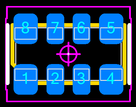
Here is Panasonic's suggested land pattern. They suggest a pattern that
does not have extra wide pads in the corners that match the part. They
make all 8 pads the same exact size. 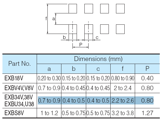
I've looked at other manufacturers and found a mix. Some are more like Library Expert and some are like Panasonic. Since Panasonic has a wide range of acceptable dimensions, I don't think it matters a lot what I choose, but I wanted to ask about the pads in the corners. Note that the pitch is 0.8mm, and the pad for dimension A1 in the picture below is off center. Library Expert properly creates an off-center pad (with respect to the pitch) and the pad is wider than the ones in the middle. 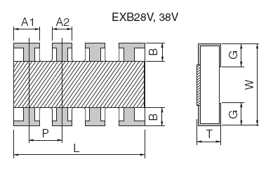
Do you know why Panasonic (and multiple others) wouldn't recommend a pattern with wider pads in the corners? What is very odd is that the Panasonic EXB2HV series is the opposite. All of its terminals are the same width, yet the land pattern has wider pads in the corners! It is a narrower pitch part (0.5mm), and I'm guessing the wider pads in the corners help to align the part and keep it from shifting during reflow? I think I'm using the word "terminal" properly. If I'm not, I mean "pin". Thanks, Greg |
|
 |
|

|
|
|
|
|
Tom H
Admin Group 

Joined: 05 Jan 2012 Location: San Diego, CA Status: Offline Points: 6070 |
Post Options
Thanks(0)
Quote Reply
Posted: 13 Feb 2019 at 8:49am |
|
I need the Datasheet web-link to validate your claim.
All I can find on Panasonic is this Chip Resistor Array Type: EXB 14V, 18V, 24V, 28V, N8V, 2HV, 34V, V4V, 38V, V8V, S8V and the datasheet does not provide any mfr. recommended patterns. Please provide enough information to validate your research. Thank you. |
|
|
|
|
gcary
Advanced User
Joined: 06 Mar 2012 Location: USA Status: Offline Points: 69 |
Post Options
Thanks(0)
Quote Reply
Posted: 13 Feb 2019 at 9:48am |
|
Here is the link to the land patterns where I got the image from: The family I'm using is EXB38V.
|
|
|
|
|
gcary
Advanced User
Joined: 06 Mar 2012 Location: USA Status: Offline Points: 69 |
Post Options
Thanks(0)
Quote Reply
Posted: 13 Feb 2019 at 9:53am |
|
Maybe you didn't see that I had edited my original post. I had copied and pasted the content from another document I was editing, and the forum software didn't complain about the images. It displayed them nicely, but after posting it, none of the images were shown. So I edited it to insert the images. If you replied to my post from your e-mail you might not have seen the edit.
|
|
|
|
|
Tom H
Admin Group
Joined: 05 Jan 2012 Location: San Diego, CA Status: Offline Points: 6070 |
Post Options
Thanks(0)
Quote Reply
Posted: 13 Feb 2019 at 10:34am |
|
Here is the Panasonic EXB28V mfr. recommended pattern. Wide end pads for wide end leads.
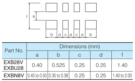 Here is the Package Dimensions. When the "A2" dimension is missing or "A1" is the same value as "A2" the End Leads are the Same Width. When "A1 and "A2" are different values (like EXB28V), the End Leads are Wider. 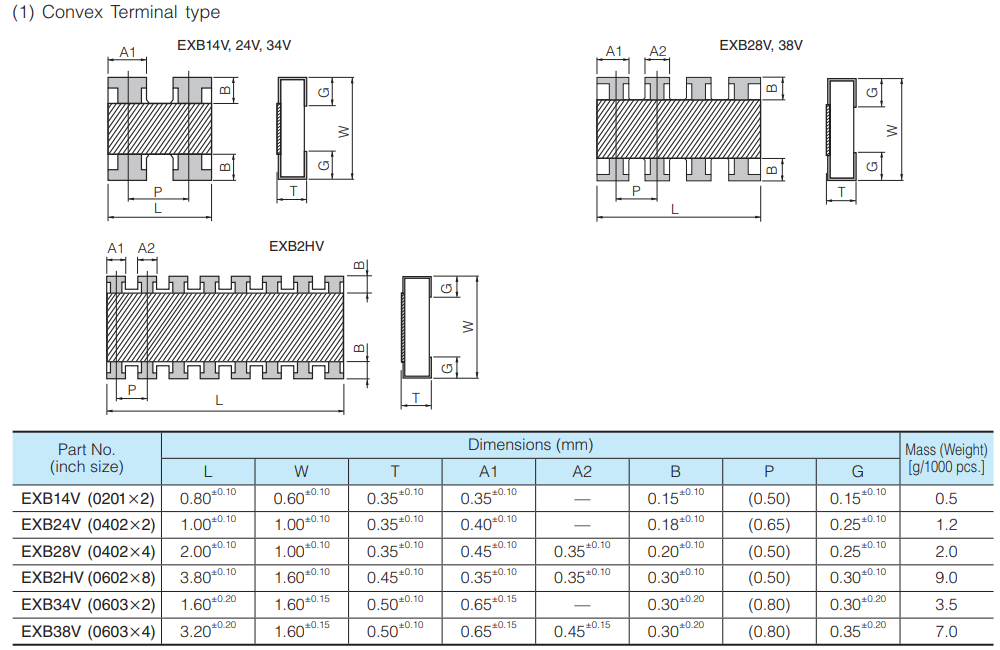 The Library Expert Chip Array Calculator has not changed in the past 7 years. I do not understand the issue that you are trying to convey. Must be a misunderstanding. |
|
|
|
|
gcary
Advanced User
Joined: 06 Mar 2012 Location: USA Status: Offline Points: 69 |
Post Options
Thanks(0)
Quote Reply
Posted: 13 Feb 2019 at 11:41am |
|
I'm using the EXB38V, not the 28V. Just to be clear, I'm not suggesting the Library Expert calculator is wrong. I am the kind of person that wants to know "why" about everything. Why is Panasonic's land pattern for the EXB38V not the same as the EXB28V? Industry experts in many seminars I've attended have said that you shouldn't trust the data sheets. Mistakes are made. And humans write the datasheets, and humans are not perfect. So what they write wouldn't need to be a mistake. It could simply be wrong. This is probably most true about layout recommendations. In this case, I don't think Panasonic made a mistake, but there must be some rationale for the dimensions they recommend. Maybe there is enough surface tension during reflow that the pads for the wide end leads don't need to be wide. The part will always remain oriented properly. This would allow a little more room for routing traces along the side of the part (I know it is a stretch, but that is all I can come up with besides they know better than IPC). Something else I didn't bring up is the width of the pads. Library Expert's recommended width for the inner pads is 0.54mm, and Panasonic's recommended range is 0.4 to 0.5. At 0.54mm, a trace would need to be 3.4 mils wide to squeeze between the pads (assuming a 3.4-mil space). At 0.5mm the trace would be about 4 mils, and at 0.4mm, the trace would be a comfortable 5.2 mils. So maybe their recommendation takes this into account. Thanks, Greg |
|
|
|
|
Tom H
Admin Group
Joined: 05 Jan 2012 Location: San Diego, CA Status: Offline Points: 6070 |
Post Options
Thanks(0)
Quote Reply
Posted: 13 Feb 2019 at 12:01pm |
|
You could be right. It might be a mfr. datasheet typo.
|
|
|
|
|
Post Reply
|
|
| Tweet |
| Forum Jump | Forum Permissions You cannot post new topics in this forum You cannot reply to topics in this forum You cannot delete your posts in this forum You cannot edit your posts in this forum You cannot create polls in this forum You cannot vote in polls in this forum |


 Topic Options