

|
|
Three Pin Ferrite Beads |
Post Reply 
|
| Author | |
DaveCowl 
Advanced User 

Joined: 18 Oct 2012 Location: Santa Clara, CA Status: Offline Points: 161 |
 Post Options Post Options
") Thanks(0) Thanks(0)
 Quote Reply Quote Reply
 Topic: Three Pin Ferrite Beads Topic: Three Pin Ferrite BeadsPosted: 25 Oct 2012 at 10:10am |
|
Has anyone dealt with the Ferrite Beads like the Murate NFE31P parts that have a barrel with a middle GND pin on a MELF like construction?  The recommended footprint from Murata is very odd and of course it defies naming conventions or standard footprint generation. The land pattern that I inherited basically looks like a 1206 with an extra pad in the middle, but that is far from the recommended shape, which is odd since the end pads are narrower than the part itself, though the end caps are round... I will try to include the footprint for reference. 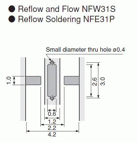 Thoughts or recommendations? Just run with the recommended land pattern?
|
|
 |
|

|
|
|
|
|
Tom H
Admin Group 

Joined: 05 Jan 2012 Location: San Diego, CA Status: Offline Points: 6074 |
Post Options
Thanks(0)
Quote Reply
Posted: 25 Oct 2012 at 10:15am |
|
I would go with the mfr. recommended pattern. The CM must have tested it on a reference design to proof it out. This package is a unique one-of-a-kind non-standard part.
It needs to be built once, built right and never built again by anyone. But we'll get there soon. |
|
|
|
|
DaveCowl
Advanced User
Joined: 18 Oct 2012 Location: Santa Clara, CA Status: Offline Points: 161 |
Post Options
Thanks(0)
Quote Reply
Posted: 25 Oct 2012 at 10:30am |
|
The strangest thing about the pattern is that the white areas are (from the best I can tell) devoid of solder mask. Which is a pretty huge solder mask opening, that is essentially 'open ended' on the top and bottom.
The solder mask pattern is the light grey.
My tendency would be to have a more typical solder mask pattern that is essentially the inverse of the pads. Perhaps the recommendation is the minimum required solder mask? I am not sure what to make of this... |
|
|
|
|
Post Reply
|
|
| Tweet |
| Forum Jump | Forum Permissions You cannot post new topics in this forum You cannot reply to topics in this forum You cannot delete your posts in this forum You cannot edit your posts in this forum You cannot create polls in this forum You cannot vote in polls in this forum |


 Topic Options