

|
|
Same chip size but different terminal metalization |
Post Reply 
|
| Author | |
dramos 
Advanced User 
Joined: 18 Feb 2021 Status: Offline Points: 101 |
 Post Options Post Options
") Thanks(0) Thanks(0)
 Quote Reply Quote Reply
 Topic: Same chip size but different terminal metalization Topic: Same chip size but different terminal metalizationPosted: 18 Feb 2021 at 2:19am |
|
Hi to all,
I have been making a small research with footprints on same resistor size. I have been working with Samsung, Vishay and Yageo. According with PCBLibraries here is the data of each component 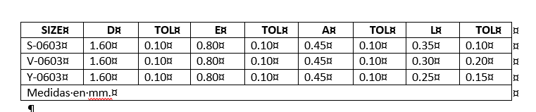 As it was supposed the size of the pads are different because the metal termiantions are different. I took Samsung and Yageo in order to see any difference between them. 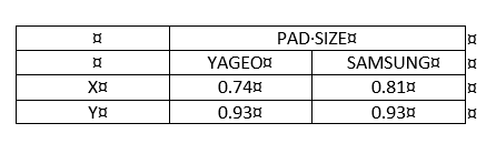 Taking the same center reference here is a comparison. The top pads are obtained using PCBL with SAMSUNG data Th ebottom pads are obtained using PCBL with YAGEO data The green body is the YAGEO resistor. The magenta body is the SAMSUNG resistor 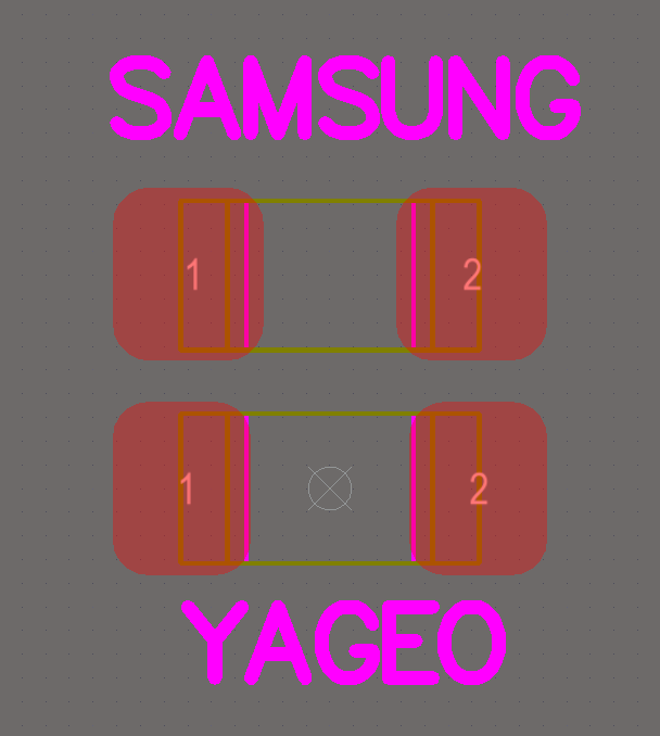 The Samsung part on the Yageo footprint is "at limit" In the other hand, the Yageo part on the Samsung footprint has a big amount of ceramic over the pad. My opinion is the the Samsung part is ok over the Yageo footprint. I would like to know your opinion about it. I know that it is impossible to have only a footprint for all resistors, caps,.... Thanks a lot for your time. Regards. David |
|
 |
|

|
|
|
|
|
Tom H
Admin Group 

Joined: 05 Jan 2012 Location: San Diego, CA Status: Offline Points: 6074 |
Post Options
Thanks(1)
Quote Reply
Posted: 18 Feb 2021 at 8:59am |
|
As long as the Terminal Lead is on the pad it will work OK.
For the Chip component family, the solder strength is under the Terminal Lead and the Toe area. The Heel only provides area for packages with different Terminal Lead Lengths. The assembly problems occur when the Terminal Lead falls off the pad. |
|
|
|
|
Post Reply
|
|
| Tweet |
| Forum Jump | Forum Permissions You cannot post new topics in this forum You cannot reply to topics in this forum You cannot delete your posts in this forum You cannot edit your posts in this forum You cannot create polls in this forum You cannot vote in polls in this forum |


 Topic Options