

|
|
Standard Chip Package Case Codes & Dimensions |
Post Reply 
|
Page 12> |
| Author | |
Tom H 
Admin Group 

Joined: 05 Jan 2012 Location: San Diego, CA Status: Offline Points: 6075 |
 Post Options Post Options
") Thanks(0) Thanks(0)
 Quote Reply Quote Reply
 Topic: Standard Chip Package Case Codes & Dimensions Topic: Standard Chip Package Case Codes & DimensionsPosted: 24 Feb 2019 at 12:33pm |
|
Chip Resistor: 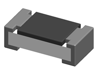 Chip Non-polarized Capacitor:  Chip Inductor:  Chip Diode: 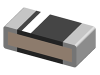 Chip LED:  Chip Antenna:  Chip Polarized Capacitor: 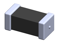 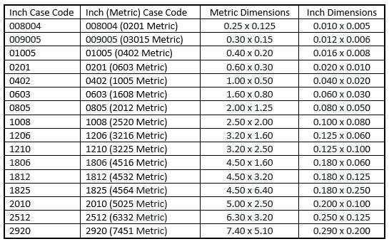 If the Chip dimensions do not match the table then a new or different Case Code must be assigned. Note: there are various Heights to all of these packages, but the Height does not impact the resulting pad size for the Footprint Land Pattern. However, the Height is important for the 3D STEP model creation and should be included in the Footprint name. Also, the Terminal Lead may be a different length and that should be included in the Footprint Name because that does affect the resulting pad size. Here is a typical Footprint Name for a 0201 (0603 Metric) Capacitor part: Footprint Land Pattern Name: CAPC60X32X27L15 CAP = Capacitor C = Chip 60 = 0.60 mm body Length 32 = 0.325 mm body Width 27 = 0.275 mm maximum Height L15 = 0.15 mm nominal Lead Length Notice that the Leading Zeros are ignored and only the first 2 numbers to the right of the decimal point is used in the Footprint Name. But the Leading zeros are in the Case Code. The Case Code = one number to the left and right of the decimal point. A typical Physical Description for this package will be: Capacitor, Chip; 0.60 mm L X 0.325 mm W X 0.275 mm H body The EIA Inch Based Names are still widely used today in the electronics industry, even though the Metric Names created by EIAJ in Japan were first introduced in the 1980's in the PDP-100 publication. American assembly shops, EE engineers and component manufacturer's did not adapt to the metric naming convention and translated all of the original documentation from Metric to Imperial units so they could better comprehend the package sizes. This was one of the biggest mistakes in the global electronics industry and very short sited of the future of the industry. Today, all Standard package dimensions are printed using Metric Dimensions but the translated Inch Based package names have deep roots in the industry and have settled as the defacto standard. Now we have to deal with 2 systems of measurement rather than the supreme metric unit measuring system. |
|
 |
|

|
|
|
|
|
Arun7290
New User 
Joined: 10 Mar 2021 Status: Offline Points: 7 |
Post Options
Thanks(0)
Quote Reply
Posted: 24 Mar 2021 at 10:01am |
|
Hi,
From the above table, Is it possible to have a standardized terminal lead length for all the packages?
|
|
|
|
|
Tom H
Admin Group
Joined: 05 Jan 2012 Location: San Diego, CA Status: Offline Points: 6075 |
Post Options
Thanks(0)
Quote Reply
Posted: 24 Mar 2021 at 11:03am |
|
The component manufacturer's will never standardize the Terminal Lead Length or the Tolerance.
|
|
|
|
|
Arun7290
New User
Joined: 10 Mar 2021 Status: Offline Points: 7 |
Post Options
Thanks(0)
Quote Reply
Posted: 25 Mar 2021 at 11:52am |
|
Hi Tom,
Thanks for the reply. Can we use the above listed package sizes for Wraparound parts as well in the same case code? Because It is mentioned that the above case code dimensions are only for Standard Chips. And I am working on some wraparound packages of the standard case code. Can we use PCB library expert for footprint creation for these parts? Or Is it better to follow the Manufacturer recommended land pattern?  |
|
|
|
|
Tom H
Admin Group
Joined: 05 Jan 2012 Location: San Diego, CA Status: Offline Points: 6075 |
Post Options
Thanks(0)
Quote Reply
Posted: 25 Mar 2021 at 11:59am |
|
Use the mfr. recommended pattern for this new upcoming component family.
Some manufacturers use a periphery solder joint goal and other use a Toe, Heel and Side pad stack. This is a new Terminal Lead form that has not been fully tested by the world standards like IPC-J-STD-001 for solder joint acceptability. |
|
|
|
|
lladam
New User
Joined: 02 Jul 2021 Status: Offline Points: 1 |
Post Options
Thanks(0)
Quote Reply
Posted: 02 Jul 2021 at 6:26am |
|
Hi,
How to make a Proteus library part of MEGA2560 Pro Mini, or where can find one please. Because the board too small to put many pins on. Thanks
|
|
|
|
|
Tom H
Admin Group
Joined: 05 Jan 2012 Location: San Diego, CA Status: Offline Points: 6075 |
Post Options
Thanks(0)
Quote Reply
Posted: 02 Jul 2021 at 8:47am |
|
You need to attach a link to a PDF file zipped or a URL link to the datasheet would be better.
Then we can post the Proteus footprint. Are you using the Free V2021 Footprint Expert Pro for Proteus? You could create the footprint in a couple minutes. |
|
|
|
|
phil.holden
Advanced User 
Joined: 14 Aug 2020 Status: Offline Points: 59 |
Post Options
Thanks(0)
Quote Reply
Posted: 07 Sep 2021 at 4:08am |
|
As is common procedure, especially during these times with supply-chain issues. We try and specify x3 MPNs for all of our passive devices.
As there could be 3 substituted parts fitted all with differing terminal lengths. How am i best addressing this when creating a passive library? This is much less of a problem for active parts and connectors that are less 'interchangeable'. Thanks In addition to the above. I have noticed that the terminals sometimes overhang the pads when using 'rounded rectangle'. In your opinion, would this be a problem? 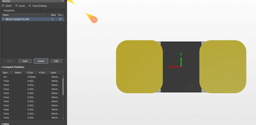 |
|
|
|
|
Tom H
Admin Group
Joined: 05 Jan 2012 Location: San Diego, CA Status: Offline Points: 6075 |
Post Options
Thanks(0)
Quote Reply
Posted: 07 Sep 2021 at 9:08am |
|
To get 3 or more passive packages to fit into the same Footprint, find parts with the same dimensions and tolerances. If the package dimensions are the same but the tolerances are different, then round the tolerances off so that they are all the same. Change this setting in "Tools > Options > Pad Stack Rules > SMD Corner Rounding > Corner Radius Limit".
|
|
|
|
|
phil.holden
Advanced User
Joined: 14 Aug 2020 Status: Offline Points: 59 |
Post Options
Thanks(0)
Quote Reply
Posted: 08 Sep 2021 at 5:26am |
|
Hi Tom,
For my Enterprise Edition CLOUD Licensed the options under Pad Stack Rules are 'greyed' out. Does this mean that i am unable to control this globally?
 |
|
|
|
|
Post Reply
|
Page 12> |
| Tweet |
| Forum Jump | Forum Permissions You cannot post new topics in this forum You cannot reply to topics in this forum You cannot delete your posts in this forum You cannot edit your posts in this forum You cannot create polls in this forum You cannot vote in polls in this forum |


 Topic Options