

|
|
QFN Thermal Via Pitch |
Post Reply 
|
| Author | |
jnbrown 
Active User 
Joined: 13 Jan 2020 Status: Offline Points: 40 |
 Post Options Post Options
") Thanks(0) Thanks(0)
 Quote Reply Quote Reply
 Topic: QFN Thermal Via Pitch Topic: QFN Thermal Via PitchPosted: 19 May 2021 at 11:57am |
|
I am not sure how best to determine the pitch for QFN thermal pads.
If I put a via in between the squares of solder paste the pitch is about 1.8mm. This is using the footprint generated from Footprint Expert. Some app notes I have read recommend a pitch of 1.0 to 1.5 mm Is there an IPC spec for this? I assume there is a way to set the size and number of solder paste squares in Footprint Expert? Thanks
|
|
 |
|

|
|
|
|
|
jnbrown
Active User
Joined: 13 Jan 2020 Status: Offline Points: 40 |
Post Options
Thanks(0)
Quote Reply
Posted: 19 May 2021 at 11:59am |
|
Here is the footprint showing the solder paste squares.
 |
|
|
|
|
Tom H
Admin Group 

Joined: 05 Jan 2012 Location: San Diego, CA Status: Offline Points: 6075 |
Post Options
Thanks(0)
Quote Reply
Posted: 19 May 2021 at 12:55pm |
|
There is an IPC-7093A standard for BTC packages and recommended patterns.
There are several controls in V2021 Footprint Expert that allow you to control the paste mask aperture sizes and openings. If you need to control the aperture size and spacing, you must move the QFN footprint to FP Designer and edit the pad stack / Paste Mask layer. In "Tools > Options > Pad Stack Rules > SMD Thermal Tabs > Thermal Tab Minimum Pattern Space" the default setting is 0.20 mm, but you can change the value to control the spacing of the checkerboard pattern. According to the IPC-7093A you can also solder mask define the thermal pad to dam in the paste mask to prevent it from flowing into via holes. This saves PCB fabrication costs because you do not need to plug the via holes. Here is a link to a forum post that has some info on IPC-7093A - |
|
|
|
|
jnbrown
Active User
Joined: 13 Jan 2020 Status: Offline Points: 40 |
Post Options
Thanks(0)
Quote Reply
Posted: 20 May 2021 at 8:53am |
|
Tom,
Thanks for the info. When I go to Tools > Options > Pad Stack Rules > SMD Thermal Tabs > Thermal Tab Minimum Pattern Space all of the options are grayed out and I cannot change them. I found the same options on the panel in the lower left and I can change them there. When I change the value Thermal Pad Minimum Pattern Space it has no effect on the solder paste pattern. This pattern has a pitch of about 1.85 mm. I don't see a way to make the pitch smaller. Here is what the footprint looks like in FP Expert: 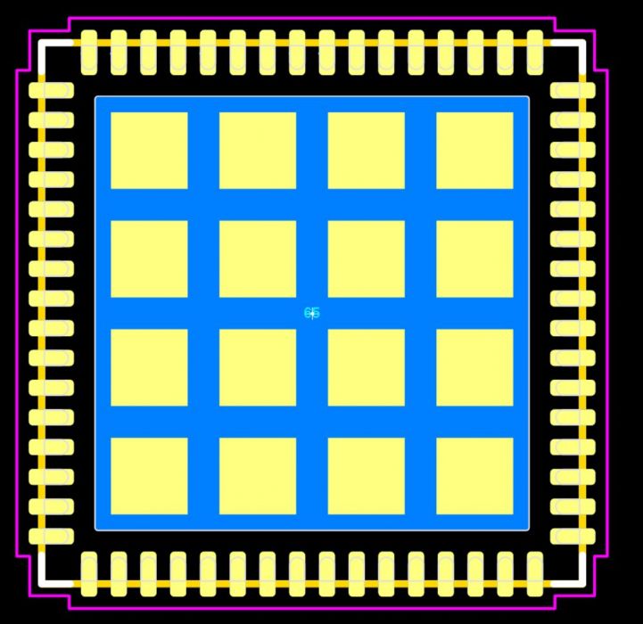 Regarding IPC-7093A and solder mask defined thermal pad, is this something that FP Expert automatically creates or do I have do it manually in Altium? -Joel |
|
|
|
|
Tom H
Admin Group
Joined: 05 Jan 2012 Location: San Diego, CA Status: Offline Points: 6075 |
Post Options
Thanks(0)
Quote Reply
Posted: 20 May 2021 at 9:02am |
|
Tools > Options > Internal Defaults cannot be edited.
You must File > Save As > your .opt file to edit over 1,000 options. You can create as many option files as you need. Some companies use 10 option files for creating footprints with different rules. There is a "Tools > Options > Pad Stack Rules > Thermal Tab" option for solder mask defining thermal pads. This feature will make the solder mask and paste mask apertures the same size. It dams in the paste mask from flowing and it reduces paste mask voiding. |
|
|
|
|
jnbrown
Active User
Joined: 13 Jan 2020 Status: Offline Points: 40 |
Post Options
Thanks(0)
Quote Reply
Posted: 20 May 2021 at 9:22am |
|
Ok, I did Save As and now I can edit the options.
But changing Thermal Pad Minimum Pattern Space still has no effect on the solder paste pattern.
|
|
|
|
|
Tom H
Admin Group
Joined: 05 Jan 2012 Location: San Diego, CA Status: Offline Points: 6075 |
Post Options
Thanks(0)
Quote Reply
Posted: 20 May 2021 at 9:32am |
|
Normally, the space between paste mask apertures is greater of 0.50 mm.
The default Option setting is 0.20 minimum which means anything greater than that will have no affect. If you select 60% paste mask coverage and enter a 0.50 minimum space, you might not get 60% coverage. Also, most component manufacturers recommend a rectangular shape thermal pad, even though the thermal tab terminal has a 45 degree chamfer. They almost never recommend corner radius on a thermal pad. A rectangle thermal pad is a Flash Aperture for Gerber data. A Chamfered or Radius thermal pad is drawn copper ploy shape and takes long to process. Let me know if you need/want a webcast demo so I can see your screen and help you with your Option settings. |
|
|
|
|
jnbrown
Active User
Joined: 13 Jan 2020 Status: Offline Points: 40 |
Post Options
Thanks(0)
Quote Reply
Posted: 20 May 2021 at 11:54am |
|
I sent this to our assembler and they are ok with it, so I am going to leave it as is.
BTW, I have discussed with them in the past about plugging the vias and they told me that they can assemble it either way but that they get a better solder joint with the vias open. There seems to be some debate about this and no consensus as to whether it is better to leave the vias or plug them. |
|
|
|
|
Tom H
Admin Group
Joined: 05 Jan 2012 Location: San Diego, CA Status: Offline Points: 6075 |
Post Options
Thanks(0)
Quote Reply
Posted: 20 May 2021 at 12:15pm |
|
What happens to the paste mask flow into via holes is that since the vias are connected to the GND planes with direct connections (no thermal reliefs), the solder cools before it goes all the way through the hole and out the back side.
Some people are concerned about avoiding problems and they do not assume anything and pay extra to plug the via holes. The 0.20 minimum paste mask gap on the checker board is just to insure that the paste stencil is rugged enough to withstand production. Stencils are expensive and thin webs break. However, the paste stencil web on a 0.40 pin pitch pattern could be smaller than 0.20. We're adding a feature in the Pad Stack Rules Options to allow the user to ensure a 0.20 minimum stencil web on all footprint patterns, but the value is user definable. |
|
|
|
|
Post Reply
|
|
| Tweet |
| Forum Jump | Forum Permissions You cannot post new topics in this forum You cannot reply to topics in this forum You cannot delete your posts in this forum You cannot edit your posts in this forum You cannot create polls in this forum You cannot vote in polls in this forum |


 Topic Options