Additional Assembly Graphics?
Printed From: PCB Libraries Forum
Category: PCB Footprint Expert
Forum Name: Questions & Answers
Forum Description: issues and technical support
URL: https://www.PCBLibraries.com/forum/forum_posts.asp?TID=969
Printed Date: 29 Mar 2026 at 3:40am
Topic: Additional Assembly Graphics?
Posted By: BennsPCB
Subject: Additional Assembly Graphics?
Date Posted: 16 Jun 2013 at 1:14am
|
A plain rectangle or circle is perhaps not the most optimal way to describe/show a component. Is there a way to add graphics (lines/text/symbols, ...) to the Assembly representation? /Benn |
Replies:
Posted By: Tom H
Date Posted: 16 Jun 2013 at 1:15pm
|
A corner chamfer by pin 1 helps if the component should not be assembled inverted. Resistors and non-polarized capacitors don't need a corner chamfer because they can be inverted during assembly. But all IC's and polarized discrete passive components need a corner chamfer because they only have 1 assembly option. But the point is right on. Assembly outlines for assembly drawings do not need to be complex shapes to show off an individual's artistic personality. They should be simple rectangle or circle because the only one who ever sees the assembly drawing is the assembly shop. Why spend a lot of time on something that no one cares about. After the assembly process or after the assembly shop automates the assembly line, the assembly drawing is archived along with the Gerber data and most of the time never seen again. However, there are some PCB designers who import DXF files with complex details of many line segments representing the physical component. They use these imported lines for both the silkscreen and the assembly drawing. Unfortunately the artistic silkscreen gets covered up by the component body during assembly so the EE engineer or the end consumer never gets to see it. So why do it? This is a real question that I need to know what is the reason to do this? To me, it makes the Footprint file size large and when you put a lot of these in your PCB layout, the file size gets large and it takes longer to post process, uses up more silkscreen ink (unnecessarily) and makes the assembly drawing size larger. All of this translates into expense for the corporation (the company you work for). Simple is better. PCB designers would be better off to use their artistic qualities on a hobby. But alas, PCB design is some people's hobby. If you have a lot of time on your hands and your company does not care about the additional expense to create complex silkscreen and assembly outlines, then go for it. |
Posted By: dwaltoneng
Date Posted: 16 Jun 2013 at 2:24pm
|
It could help during layout to have a bit more detail on some components. For example: Side activated switches. For connectors designed to hang over the edge of the board, it is useful to have a marker for the board edge. Large complex shape components, eg pressure sensors with spigots for pressure tubing. |
Posted By: Tom H
Date Posted: 16 Jun 2013 at 2:45pm
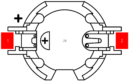
You're correct. I was referring to parts like this SMT speaker. This silkscreen outline does not help the PCB designer, fabrication or assembly process. And it's covered up after assembly except the "+".  |
Posted By: BennsPCB
Date Posted: 16 Jun 2013 at 11:35pm
|
I see your point Tom, and in the case of silkscreen I totally agree, but I haven't mentioned silkscreen in my question. I was referring to how to slightly improve the Assembly drawing, that is (still) used not only by prototype assembly people but also the guys that have to repair in the fields. A simple line/box/triangle/circle/text would certainly help to clarify in many cases, without adding too much complexity/info to the footprint data. That SMT speaker example is way too complex and is absolutely NOT what I would prefer. /Benn |
Posted By: jameshead
Date Posted: 17 Jun 2013 at 12:31am
|
It's useful to have something a bit more representative sometimes on both silkscreen and assembly diagrams for hand inserted components. Operators will use both silkscreen on the board and the assembly drawing. |
Posted By: rdl86626
Date Posted: 17 Jun 2013 at 7:27am
| I agree. I have been adding polorization symbols to diodes and caps and pin 1 of chips because the assembly drawing may not be available to test techs. Everyone here wants it to be more visable. |
Posted By: matthelm
Date Posted: 21 Jun 2013 at 9:56am
|
First, these comments are for production boards. If you are just doing low run boards, add all the detail you want/have time for, as your assembly process may have NO automation, and then you just might need all that stuff. The only time I add extra to the assembly, is if it helps place/ID the part. If I get the DXF Tom has above, I'd remove about 95% of the details. I'd leave the outer edge, and the internal "+", maybe the internal circle and the some of the pin details, depending on if it helps get the part placed correctly. I never add anything to the silk, except the outline (MAX size) and the polarity marker. BTW, if you are making a larger number of boards (3K/Month or more) you can save a bit by removing the silk from production boards, but if you do, make sure everyone can get to the assembly drawings. A company I worked for in the 90s did this, and had no issues, and with the parts getting smaller and smaller .... |