Proportional Through-hole Padstacks
Printed From: PCB Libraries Forum
Category: Libraries
Forum Name: PCB Library Construction Guidelines
Forum Description: Documentation of the Footprint Expert Guidelines
URL: https://www.PCBLibraries.com/forum/forum_posts.asp?TID=90
Printed Date: 26 Jun 2026 at 9:00am
Topic: Proportional Through-hole Padstacks
Posted By: Nick B
Subject: Proportional Through-hole Padstacks
Date Posted: 14 Mar 2012 at 3:22am
|
Here is the latest Through-hole Padstacks file - Updated 8-9-12 http://www.pcblibraries.com/downloads/Guidelines!Proportional_Through-hole_Padstacks.asp" rel="nofollow - DOWNLOAD (you need to be logged in, registration is absolutely free!)
|
Replies:
Posted By: Chris
Date Posted: 14 Mar 2012 at 4:29am
|
Thanks very much. |
Posted By: Nightwish
Date Posted: 14 Mar 2012 at 6:56am
|
Thanks a lot for sharing this with us |
Posted By: Nick B
Date Posted: 15 Mar 2012 at 3:38am
Updated on March 15, 2012 - see link in original post for latest version.
|
Posted By: IanOnBass
Date Posted: 15 Mar 2012 at 2:08pm
| Excellent resource. Thanks for sharing. |
Posted By: RLS2004
Date Posted: 15 Mar 2012 at 2:37pm
| Thanks for updating TH Padstacks. |
Posted By: Taylor_RS
Date Posted: 16 Mar 2012 at 5:56am
| Thanks a ton! |
Posted By: Artwork Master ITALY
Date Posted: 18 Mar 2012 at 9:51am
| Great work! |
Posted By: Nick B
Date Posted: 20 Mar 2012 at 2:40am
|
The link above was updated again: Updated the Thermal Spoke Width calculations for Plated Through Hole padstacks The new improved formula is: Spoke Width = 75% of Plane Anti-pad divided by 4 |
Posted By: Tom H
Date Posted: 20 Mar 2012 at 11:15am
|
Here is the "Proportional Through-hole Padstack" Mathematical Model data: The first column is the Maximum Component Lead Size and it is determined by - 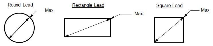 The second column is the Finished Hole Size and it is determined by adding 8 mil (0.2 mm) to the Maximum Lead Size in the first column. This is the "Nominal" Lead to Hole calculation as seen in the chart from the IPC-2222 standard.  The next 5 columns are the Pad Sizes for all the layers and they are the same value across all the rows. The Pad Size starts out using the IPC-2221 nominal annular ring requirements of 10 mil (0.25 mm) or the Pad is 20 mil (0.5 mm) larger than the hole size. Then, as the hole size gradually gets larger, the pad annular ring grows "Proportionally" larger in increments of 1 mil (0.025 mm). The primary theory is that the hole size gets larger to accommodate a larger component lead. Larger component leads are created to carry additional current or because the component size is large and needs stronger support (more solder). The Plane Anti-Pad Clearance is derived from the Hole Size and it remains relatively constant because it has nothing to do with supporting large components. It's simply a clearance from the hole to improve the PCB manufacturing yields. The minimum annular ring of the Plane Anti-Pad is 15 mil (0.35 mm) for holes intended for component leads. As the hole size grows in size, the Plane Anti-Pad stays somewhat constant but it does slightly grow as the hole size grows to keep a safe distance from higher voltage currents that larger holes can carry. The Thermal Relief is a simple formula - The ID is 20 mil (0.5 mm) larger than the Hole Size The OD is the same value as the Anti-pad The Spoke Width = Anti-pad X 75% divided by 4 spokes, the calculated spoke width X 4 = Hole Size or slightly larger than the hole |
Posted By: zasanil
Date Posted: 21 Mar 2012 at 9:56am
| Thanks a bunch for sharing this great resource. |
Posted By: kmoyer72
Date Posted: 21 Mar 2012 at 1:40pm
| thanks |
Posted By: konraditen
Date Posted: 26 Mar 2012 at 5:25pm
|
Appreciate the work that was put in. Thank you. K |
Posted By: Nellie44Militello
Date Posted: 01 Aug 2012 at 1:01pm
I was just browsing for relevant posts for my http://www.bittele.com/low-volume-pcb-assembly.asp" rel="nofollow - small volume pcb assembly project and I happened to stumble
upon yours. thanks for this useful link. it's appreciated. dave
|
 Nick B wrote:
Posted By: budnoel
Date Posted: 02 Aug 2012 at 10:07am
|
There doesn't appear to be any differentiation regarding density level in this new chart. Am I missing something? |
Posted By: Tom H
Date Posted: 02 Aug 2012 at 10:35am
|
The IPC-7251 for through-hole component package land pattern footprints has not been released yet. I really don't know why IPC is taking so long. PCB Libraries, Inc. developed the Proportional Through-hole Padstack Chart which takes into consideration all 3-Tiers in a single solution. Small hole sizes use the Least Environment for the annular ring. Average hole sizes use the Nominal Environment annular ring and larger hole sizes use the Most Enviroment annular ring. Where as IPC-7251 uses the same annular ring for each environment regardless of how big the hole size is. Example: The IPC-7251 annular ring for Nominal Environment is 10 mil (0.25 mm) regardless if the hole size is 30 mil (0.76 mm) or 98 mil (2.5 mm). The proportional padstack uses a 10 mil (0.25 mm) annular ring for 30 mil (0.76 mm) hole, but the 98 mil (2.5 mm) hole has a 25 mil (0.635 mm) annular ring. PCB Libraries, Inc. position is that large holes require large annular rings for more solder but also to control heat dissipation. So the Proportional Padstack Chart meets or beats IPC-7251 standards. We will release the through-hole component families on August 11 and the user will be able to select from IPC-7251 3-Tier or use the Proportional padstack (which is the PCB Footprint Expert) default. |
Posted By: hawesa
Date Posted: 21 Aug 2012 at 7:55am
|
Hi all,
Could you explain how the VIA padstack dimensions are calculated in the padstack chart?
They appear to follow a different formula to the PTH component Padtacks, unless I'm missing something!
e.g. a Level B padstack with a FHS of 0.4mm has a pad size of 1.00mm whilst in the VIA chart, a 0.4mm hole has a pad size of between 0.65mm and 0.8mm.
I realise there is no solder fillet required on a via but have been tearing what little there is left of my hair out trying to figure out how the VIA pad is calculated and if it is defined anywhere in IPC!
|
Posted By: Tom H
Date Posted: 21 Aug 2012 at 8:20am
|
Vias are not specified in any IPC standard. A through-hole that needs to support a component lead is totally different than a hole that does not ever have a component lead in it. A through-hole via simply needs to conduct current. |
Posted By: hawesa
Date Posted: 21 Aug 2012 at 8:30am
| I am trying to define a set of standard or default vias to be used by the layout team here and was intending to use the chart as a starting point but I need to understand how the values are calculated. We do not allow any breakout (worst case tangency) so how do we ensure the default vias provide for this? |
Posted By: jameshead
Date Posted: 21 Aug 2012 at 8:43am
|
I've brought this up before with Tom. Like Hawesa, I've always used the standard IPC calculations for vias as well, as have a number of designers I've worked with, but then again I've also worked with a handful of designers who've thought the same as Tom. I tried to clarify it with the IPC and got the answer back that the standard does cover vias as well as through-hole pads but other IPC people I've spoken to have thought the opposite. I think it certainly needs some clarification. I don't know if the IPC have looked at this recently and revised it? Currently I'm sticking with the IPC calculations for vias just for consistancy but I'd be perfectly happy to use the PCB Libraries padstacks for vias if the IPC updated the standard. |
Posted By: jameshead
Date Posted: 21 Aug 2012 at 8:49am
| I've mentioned this on the SMART group e-mail list as well. A good PCB fabricator mentioned that using laser direct imaging can accommodate a 0.075 mm radial annular ring for drilled hole diameter (not finished hole diameter) on an outer layer for "no breakout" condition but would recommend 0.125 mm radial for inner layers in the same pad stack. |
Posted By: Tom H
Date Posted: 21 Aug 2012 at 9:10am
|
I have heard from Gary Ferrari at this years IPC APEX conference that the IPC-2221 and 2222 are being overhauled and will be released before the next IPC APEX conference in San Diego, CA in early 2013. But I don't see any release notification here - http://www.ipc.org/CommitteeDetail.aspx?Committee=D-31B" rel="nofollow - http://www.ipc.org/CommitteeDetail.aspx?Committee=D-31B All I can say is that the Proportional Via Padstacks have been used in production by CADPRO on over 2,000 PCB layouts and Wind River (now Intel) and all their PCB Layouts before we released it to the public in 2004 via PCB Libraries, Inc. No fabrication shop or EE engineer has ever complained of problems and many of the designs we did went into high volume production. Download the paper on PCB Design Optimization Starts in the CAD Library - http://www.pcblibraries.com/forum/pcb-library-optimization-presentation-free_topic468.html" rel="nofollow - http://www.pcblibraries.com/forum/pcb-library-optimization-presentation-free_topic468.html Here is a picture from the presentation regarding inner layer shifting & annular ring - 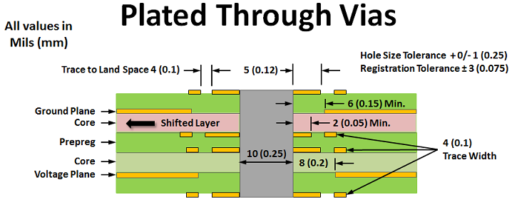 |
Posted By: plinder
Date Posted: 01 Oct 2012 at 10:43am
| The Footprint names for Mounting Holes look different than the last version of LP Wizard. What naming convention do you plan on carrying forward for Mounting Holes? |
Posted By: Tom H
Date Posted: 01 Oct 2012 at 11:54am
|
Mounting Holes will not make it into the PCB Footprint Expert. All ANSI and ISO Mounting Holes will be available in every CAD format for free download soon. |
Posted By: Vladimir.Stoyanov
Date Posted: 01 Oct 2012 at 11:41pm
|
Hi Tom, |
Posted By: Tom H
Date Posted: 02 Oct 2012 at 7:23am
|
The PCB Footprint Expert supports the unreleased IPC-7251 through-hole standard but I prefer "Proportional Padstacks" because they cover all 3-Tiers. The IPC-7251 has fixed annular rings for each tier, regardless of the hole size. The Proportional Padstack annular ring gradually increases with the hole size. So small holes use the Least annular ring, medium size holes use Nominal annular ring and larger hole sizes use the Most annular ring. Then there's a point where the hole size is larger than 2 mm (80 mils) and the annular ring gradually gets even larger than the IPC-7251 standard. So Proportional Padstacks meet or beat IPC-7251. The theory is simple. If a through-hole component lead has a large diameter it's for a reason. It might need to carry a lot of current or the component may be tall and requires stability or the component may be heavy and require support. All of these reasons require a larger annular ring which allows more solder. Example: in the case of a large component lead that carries current, this will increase the temperature as the board functions and the large annular dissipates heat. If you use the Least Environment with the small annular ring, it's less solder and less heat dissipation. Note: I've used the Proportional Padstacks on over 1,000 PCB layout designs for both prototype and production boards and never had a manufacturing problem or a field problem. It's proven to be a very reliable padstack. Here is the IPC-7251 table for Axial Lead components:  |
Posted By: Vladimir.Stoyanov
Date Posted: 02 Oct 2012 at 11:49pm
|
Dear Tom, I made terrible mistake - for PTH I use Most level, not Least. Even with this level I receive a mumble from our plants. For PTH footprints I use Excel table from PCB Matrix, but it is quite old. Do you have an update of this table? Thanks a lot! |
Posted By: Tom H
Date Posted: 03 Oct 2012 at 7:01am
|
All of the latest updated tables, charts and rules are for free download here - http://www.pcblibraries.com/forum/pcb-library-construction-guidelines_forum30.html" rel="nofollow - http://www.pcblibraries.com/forum/pcb-library-construction-guidelines_forum30.html Or here - http://www.pcblibraries.com/Downloads/" rel="nofollow - http://www.pcblibraries.com/Downloads/ |
Posted By: Vladimir.Stoyanov
Date Posted: 03 Oct 2012 at 9:46pm
|
uploads/60/IPC-7251_Padstack_Charts.xls" rel="nofollow - IPC-7251_Padstack_Charts.xls Dear Tom, Now I see that I can attach a file. I just asked you for update of this table. I don't want to use Least neither Nominal level for PTH. Can you help me? Kind regards, |
Posted By: Nick B
Date Posted: 04 Oct 2012 at 3:26pm
|
Please download the latest PTH Padstack Reference Calculator from http://www.pcblibraries.com/forum/forum_posts.asp?TID=596" rel="nofollow - HERE . |
Posted By: laiDennis
Date Posted: 23 Sep 2016 at 12:45am
 Thanks a lot for sharing this with us Thanks a lot for sharing this with us
|