Is There a Way To Go Back to LP Wizard Silkscreen?
Printed From: PCB Libraries Forum
Category: PCB Footprint Expert
Forum Name: Questions & Answers
Forum Description: issues and technical support
URL: https://www.PCBLibraries.com/forum/forum_posts.asp?TID=790
Printed Date: 14 Mar 2026 at 4:42pm
Topic: Is There a Way To Go Back to LP Wizard Silkscreen?
Posted By: Alphatronique
Subject: Is There a Way To Go Back to LP Wizard Silkscreen?
Date Posted: 08 Jan 2013 at 8:07pm
|
Hi i see that it have a 7351B.dat ,but did it have a way to got back old style silkscreen output as it was whit older "B" ? "personally" i like to see orientation marking under package ,it easy to see when program pick&place and or rework ,and still keep a small dot if need post assembly and also when work on old design and add new part you have 2 different "standard" and not to forgot pin 1 position change that screw machine programming scrip .. so think it may good to have check-box or else for got to older style Best regard Marc L. |
Replies:
Posted By: Tom H
Date Posted: 08 Jan 2013 at 8:15pm
|
Here
are the basic IPC-7351C silkscreen rules – 1.
No
silkscreen outline under the component; these get covered up during assembly
and don’t provide any useful purpose (waste of expensive inkjet cartridges) 2.
All
silkscreen outlines visible after assembly process and provide a functional use
as alignment marking for assembly registration accuracy 3.
All
silkscreen outlines must be inside placement courtyard 4.
All
Silkscreen outlines are mapped to the Maximum Component Body with 1 exception,
the Silkscreen to Pad spacing rule “overrides” the Component Body Mapping. 5.
Silkscreen
outlines should map the component body and not go around pads. Excess
silkscreen outlines should be avoided to make room for ref des locations.
Silkscreen outlines should perform a “hatch” outline along the component
package body. 6. Pin 1 is identified by extending the silkscreen along Pin 1 length to indicate polarity when the package cannot be placed inverted (inverted parts include non-polarized 2-pin parts) |
Posted By: Mattylad
Date Posted: 10 Jan 2013 at 2:45pm
What does:
mean? ISTR Hatched outlines indicates it is mounted on the other side of the board or removable. |
Posted By: Tom H
Date Posted: 10 Jan 2013 at 2:58pm
|
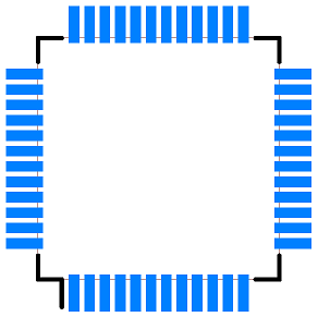
The silkscreen outline defines the component package body and does not go near or around any pads. So the Silkscreen Hatch Marks would only appear where the component body is and no component leads. However, the silkscreen outline does extend to identify Pin 1 location. An example is a simple Quad Flat Package. The brown line = the max component body outline. The silkscreen does not go around or near any pads except Pin 1. The silkscreen outline is referred to as Crop or Hatch marks. It's a USA term.  |
Posted By: Alphatronique
Date Posted: 11 Jan 2013 at 8:26am
|
Hi Tom i read whit great attention the new 7351C proposal and make some test on some specific footprint and still personally not ready yet to move to new 7351C so still think it may great to have both old and new style for silk option on footprint expert  Best regard and you make great work Marc L. |
Posted By: Tom H
Date Posted: 11 Jan 2013 at 8:50am
|
We'll be releasing a new module called the "Footprint Designer" to automate non-standard parts or even standard parts too. You will be able to build any PCB Library part in the industry. Through-hole, Surface Mount, SMT/PTH mix, 50,000 connectors and switches, relays, trim pots, transformers, etc. Our new "Footprint Designer" will allow you to quickly recreate any component mfr. recommended footprint. We're also adding 3D STEP model technology soon. I'm sure that you will like the upcoming updates in 2013. |
Posted By: BennsPCB
Date Posted: 15 Jun 2013 at 9:03am
|
When will the "Footprint Designer" be released? /Benn |
Posted By: Tom H
Date Posted: 15 Jun 2013 at 9:21am
|
The "Footprint Designer" was created for the V2013 release. V2013.04 is the next release that adds even more features. It should be released by Monday 6/17/13 However, Footprint Designer is non-functional in the free "PCB Library Expert Lite" version. |
