IPC-7351 SMD & PTH Reference Calculators
Printed From: PCB Libraries Forum
Category: Libraries
Forum Name: PCB Library Construction Guidelines
Forum Description: Documentation of the Footprint Expert Guidelines
URL: https://www.PCBLibraries.com/forum/forum_posts.asp?TID=785
Printed Date: 26 Jun 2026 at 4:48am
Topic: IPC-7351 SMD & PTH Reference Calculators
Posted By: Nick B
Subject: IPC-7351 SMD & PTH Reference Calculators
Date Posted: 07 Jan 2013 at 2:35pm
|
Here are the latest Reference Calculators. Please note there are TWO (2), one is Surface Mount, and the other Plated Through Hole, also referred to as TH. (you need to be logged in, registration is absolutely free!) http://www.pcblibraries.com/downloads/FPX!PCB_Library_Expert_SMD_Reference_Calculator.asp" rel="nofollow - IPC-7351 SMD Reference Calculator Below is the is the PCB Library Expert PTH Reference Calculator: http://www.pcblibraries.com/downloads/FPX!PCB_Library_Expert_PTH_Reference_Calculator.asp" rel="nofollow - IPC-7351 PTH Reference Calculator  ------------- Stay connected - follow us! https://twitter.com/PCBLibraries" rel="nofollow - X - http://www.linkedin.com/company/pcb-libraries-inc-/" rel="nofollow - LinkedIn |
Replies:
Posted By: jk-999
Date Posted: 02 Apr 2014 at 9:00am
|
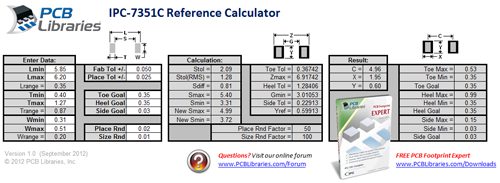
Which equation is correct? Zmax=Lmin +2JT + SQRT((CL)² + (2*F)² + (2*P)²) or
Zmax=Lmin +2JT + SQRT((CL)² + (F)² + (P)²)
IPC 7351A uses the second equation. I believe the calculator is using the first equation.
|
Posted By: Jeff.M
Date Posted: 02 Apr 2014 at 12:44pm
|
Both are correct. The difference is due to the definitions of the 'Placement' (P) and 'Fabrication' (F) tolerances. IPC-7351 demonstrates them as a single value. For example in their publication they use 0.10 mm for F and 0.20 mm for P (this is your 2nd equation). We use plus-or-minus values where an equivalent F would be +/- 0.05 mm and P would be +/- 0.10 mm so they're doubled before squaring (this is your 1st equation). Either way, the tolerances are the same and the result is the same.
------------- Stay connected - follow us! https://twitter.com/PCBLibraries" rel="nofollow - X - http://www.linkedin.com/company/pcb-libraries-inc-/" rel="nofollow - LinkedIn |
Posted By: Nick B
Date Posted: 20 Oct 2014 at 12:53pm
|
Please note the IPC-7351 Reference Calculator was just updated! There is now an Inserted Mount "IMD" (TH) Reference Calculator. Download it from this forum thread, or from http://www.PCBLibraries.com/downloads" rel="nofollow - www.PCBLibraries.com/downloads Nick ------------- Stay connected - follow us! https://twitter.com/PCBLibraries" rel="nofollow - X - http://www.linkedin.com/company/pcb-libraries-inc-/" rel="nofollow - LinkedIn |
Posted By: KevinA
Date Posted: 24 Oct 2017 at 12:22pm
|
Downloaded the Calculator and tried it but I must be doing something wrong or my math is punked: From TAIYO YUDEN:  I added B+A+B = L for Min and MAX  and ended with this:  Thanks |
Posted By: Tom H
Date Posted: 24 Oct 2017 at 12:36pm
|
You need to adjust the Toe & Heel values. The Chip component does not have a 0.35 mm Toe and Heel. Download the PCB Libraries Solder Joint Goal tables here - https://www.pcblibraries.com/account/user/memberdownloads.asp" rel="nofollow - https://www.pcblibraries.com/account/user/memberdownloads.asp ------------- Stay connected - follow us! https://twitter.com/PCBLibraries" rel="nofollow - X - http://www.linkedin.com/company/pcb-libraries-inc-/" rel="nofollow - LinkedIn |
Posted By: KevinA
Date Posted: 24 Oct 2017 at 3:01pm
|
That made a differance (User data in the WHITE fields :)) but I still ended up with a .62 for pitch meaning .38 gap between the pads of a device who's overall length is .25, they don't have a diamensional tolerance until type 063. Toe=0.05 heel=-0.03 side=-0.03 The other thing I've noticed is the manufactures have smaller pads with no side compared to any version of IPC-7351, unless they are Kemet, Kemet uses IPC-7351 but no version shown. |
Posted By: Tom H
Date Posted: 24 Oct 2017 at 3:11pm
|
The Rectangular End Cap Side Goals need to be addresses in 7351 because Resistors only have metal Terminals on 3 sides and do not (cannot) have a side fillet. But Chip Capacitors have metal Terminals on 5 sides and a side fillet is a reality. IPC-7351 is no longer a Standard (even though the cover of IPC-7351B says so). IPC-7351 is now a "Guideline" and should be used as such. Land Pattern pad size and spacing are flexible and not rigid hard core values. The IPC-J-STD-001 Standard for solder joint goal acceptability is the ruling standard for Land Patterns and it has a higher priority over IPC-7351. PCB Libraries "Library Expert V2017" solder joint goals for Toe, Heel and Side values reflect IPC-J-STD-001 and not IPC-7351B. ------------- Stay connected - follow us! https://twitter.com/PCBLibraries" rel="nofollow - X - http://www.linkedin.com/company/pcb-libraries-inc-/" rel="nofollow - LinkedIn |
Posted By: IainSynaptive
Date Posted: 26 Jan 2018 at 2:32pm
|
Good evening and Thank you for Everything you've created here! I have simple a question regarding Chip components and Circular Pads: Are they acceptable? I've been unable to locate any published Pros/Cons to this method and PC-7351B doesn't offer any guidelines to this practice. Are you able to provide any insight? Thank you in advance, |
Posted By: Tom H
Date Posted: 26 Jan 2018 at 2:55pm
|
IPC-7351 has no recommendation on using circular pad shape for Chip Components. The best source for this recommendation would be the Assembly Shop source that you are currently using. ------------- Stay connected - follow us! https://twitter.com/PCBLibraries" rel="nofollow - X - http://www.linkedin.com/company/pcb-libraries-inc-/" rel="nofollow - LinkedIn |
Posted By: dfournier
Date Posted: 09 Jul 2018 at 12:09am
|
Hello guys, I start to create footprints with IPC-7351. Could you tell me what are Thermal ID and Thermal OD for PTH?
|
Posted By: Tom H
Date Posted: 09 Jul 2018 at 7:32am
|
Thermal Relief is for all PTH pins that connect to a Plane. A PTH lead with a direct connection to a GND or VCC Plane can have a cold solder joint because the plane can dissipate all the heat from that connection. OD = Outside Diameter of Plane Pad The thermal ID & OD are connected with Spokes from the pad to the copper plane. 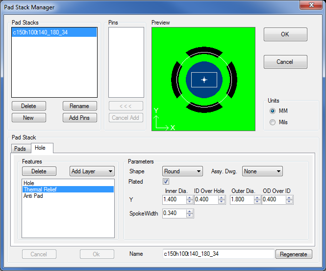 ------------- Stay connected - follow us! https://twitter.com/PCBLibraries" rel="nofollow - X - http://www.linkedin.com/company/pcb-libraries-inc-/" rel="nofollow - LinkedIn |
Posted By: dfournier
Date Posted: 10 Jul 2018 at 5:24am
|
Hello Tom, Thank you for informations. Does IPC define Thermal ID and OD? I don't find explanation that define these diameters. I use CADSTAR software and Thermal ID and OD are differently defined.  |
Posted By: Tom H
Date Posted: 10 Jul 2018 at 7:35am
|
IPC-2221 and IPC-2222 are the only documents with through-hole pad stack info. IPC-7351C is stalled in committee and will not be released for another year or so. Every CAD tool defines Thermal Relief patterns differently. Library Expert has over 100,000 users worldwide and no one has ever complained about this issue in the past 6 years. We use best practice math that we have tested and tried in a CAD tool library since 1982. ------------- Stay connected - follow us! https://twitter.com/PCBLibraries" rel="nofollow - X - http://www.linkedin.com/company/pcb-libraries-inc-/" rel="nofollow - LinkedIn |
Posted By: stanleycayochok
Date Posted: 15 Feb 2021 at 9:14pm
|
There is a difference on the Smax[RMS] formula between IPC7351 and from the "PCB Library Expert SMD Reference Calculator.xlsx" IPC7351 RMS Smax formula: Smax[RMS] = Smin + Stol[RMS] Library Expert RMS Smax formula: New Smax = Smax - (Stol -Stol[RMS])/2 Both will result in a different output value. May I know why Library Expert used such formula? |
Posted By: Jeff.M
Date Posted: 16 Feb 2021 at 11:10am
|
I believe the formula you're referring to (Smin + Stol[RMS]) dates back to the IPC-SM-782 document from 1993. IPC revised this about 2005. Please refer to IPC-7351B section 3.1.1 (should be page 11) shown as follows. This example is demonstrated in our free SMD Reference Calculator for Excel. ------------- Stay connected - follow us! https://twitter.com/PCBLibraries" rel="nofollow - X - http://www.linkedin.com/company/pcb-libraries-inc-/" rel="nofollow - LinkedIn |
Posted By: stanleycayochok
Date Posted: 25 Feb 2021 at 5:17am
|
Hi Jeff, There is no image on your post. I was referring to this Smax[RMS] formula in the 2005 IPC7351, please refer to attached image:  In the "SMD Reference Calculator for Excel" the formula is this: New Smax = Smax - (Stol -Stol[RMS])/2 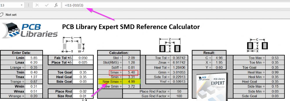 |
Posted By: Jeff.M
Date Posted: 25 Feb 2021 at 11:18am
|
You should try to get a more recent copy of IPC7351. What follows is a direct quote from IPC-7351B, June 2010. Note the line for Smax. (All the values in the Excel Reference Calculator match the example given in that document, allowing for rounding). "Therefore, the calculations for ‘‘S’’ minimum and maximum dimensions are as follows: Smin = Lmin - 2Tmax = 5.8 mm - 2 (1.27 mm) = 3.26 mm Smax = Lmax - 2Tmin= 6.2 mm - 2 (0.4 mm) = 5.40 mm Stol = Smax - Smin = 5.4 mm - 3.26 mm = 2.14 mm" Section 3.4.1 discusses the reason for creating New_Smax. New_Smax is ultimately used to produce Gmin. Not Smax. ------------- Stay connected - follow us! https://twitter.com/PCBLibraries" rel="nofollow - X - http://www.linkedin.com/company/pcb-libraries-inc-/" rel="nofollow - LinkedIn |
Posted By: stanleycayochok
Date Posted: 26 Feb 2021 at 12:47am
|
Will definitely get the latest version. Thank you Jeff for the detailed explanation.
|
Posted By: Aaronbat
Date Posted: 12 May 2023 at 4:46pm
|
Hello, I have the calculator but I'm new reviewing this kind of stuff, from where I can get the information is question on the fields:
Some of them I don't know what it means.
 |
Posted By: Tom H
Date Posted: 13 May 2023 at 8:16am
|
There is documentation on your computer in this folder: C:\Program Files (x86)\PCB Libraries\Footprint Expert 23\Documents
Read them. ------------- Stay connected - follow us! https://twitter.com/PCBLibraries" rel="nofollow - X - http://www.linkedin.com/company/pcb-libraries-inc-/" rel="nofollow - LinkedIn |
Posted By: Muhammad Faizan Ahmed
Date Posted: 22 Sep 2023 at 11:00am
| Kindly the excel sheet password |
Posted By: Tom H
Date Posted: 22 Sep 2023 at 11:20am
|
The math formulas are in the Formula toolbar.
Why do you want the password to unlock the IPC reference calculator.? ------------- Stay connected - follow us! https://twitter.com/PCBLibraries" rel="nofollow - X - http://www.linkedin.com/company/pcb-libraries-inc-/" rel="nofollow - LinkedIn |