IPC-7351 Mounting Hole Naming Convention & Info
Printed From: PCB Libraries Forum
Category: Libraries
Forum Name: PCB Library Construction Guidelines
Forum Description: Documentation of the Footprint Expert Guidelines
URL: https://www.PCBLibraries.com/forum/forum_posts.asp?TID=619
Printed Date: 26 Jun 2026 at 12:05am
Topic: IPC-7351 Mounting Hole Naming Convention & Info
Posted By: Tom H
Subject: IPC-7351 Mounting Hole Naming Convention & Info
Date Posted: 13 Feb 2013 at 1:31pm
|
Let's break it down like IPC would - MTG - component family P - Plated + pad Size - value in millimeters (2 places to each side of decimal point and drop leading zero's) NP - Non-plated + pad Size - value in millimeters (2 places to each side of decimal point and drop leading zero's) H + hole size - value in millimeters K + keepout size - value in millimeters (this normally maps to the placement courtyard diameter) V + Number of vias _ via hole size (this is a modifier and not necessary when there are no vias) T - Tight Fit L - Loose Fit Example: MTGNP1000H360K1050L We need to think of all the options and how they need to be arranged. ------------- Stay connected - follow us! https://twitter.com/PCBLibraries" rel="nofollow - X - http://www.linkedin.com/company/pcb-libraries-inc-/" rel="nofollow - LinkedIn |
Replies:
Posted By: JZsori
Date Posted: 13 Feb 2013 at 2:08pm
| OK - but in my case I will likely simplify it some. My placement courtyard will be slightly larger than the pad size. I will put in actual keepout areas as mine is a little more complicated in that I have different keepout areas for primary and secondary sides. |
Posted By: Tom H
Date Posted: 13 Feb 2013 at 2:39pm
Don't forget that all non-plated mounting holes still need a pad to support the hardware:  Here is a Mounting Hole with a Keepout: 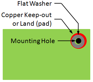 Here is Mounting Hole with sattelite support vias. The vias are usually connected to the ground plane.  Here is a Non-plated hole example: 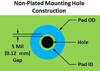 |
Posted By: Dale
Date Posted: 13 Feb 2013 at 3:20pm
|
Tom, in your last image you show a copper-free annulus between pad and hole. However I consider a non-plated mounting hole as analogous to every hole on a single-sided board - and we don't provide a copper-free annulus on those. Can you educate me/us on the differences? Thanks. |
Posted By: Tom H
Date Posted: 13 Feb 2013 at 3:25pm
|
The non-plated hole drill bit cannot hit any copper (metal), just a clean hole through the FR4 material. The mfr. desmears plated holes, but non-plated holes are plugged or masked during the plating process. IPC has a rule on this and I think it's in the newly released IPC-2221B standard (which I don't have yet, but I'll get it at APEX next week. |
Posted By: JZsori
Date Posted: 13 Feb 2013 at 3:28pm
| My understanding is that it is preferable to have a donut pad for the screw head so that the screw does not crush the epoxy glass material as much as it has a copper pad in between. |
Posted By: Dale
Date Posted: 13 Feb 2013 at 4:56pm
But why? The plated hole drill bit hits copper on every hole.
The copper pad might help distribute the force, but I don't see how this has anything to do with keeping the copper away from the hole. |
 Tom H wrote:
Posted By: Tom H
Date Posted: 13 Feb 2013 at 6:22pm
|
Both statements are correct. 1. Donut Pad so that the pad center is pulled away from the drill bit so the drill does not go through metal to avoid metal fragments and produce a clean hole. Like I mentioned, there is an excellent reason and description of the non-plated mounting hole in the newly released IPC-2221B. 2. The Donut Pad acts as mechanical support during the torque process when tightening the screw to the board to prevent the FR4 glass from crushing. i.e.: It's best to have metal on metal and avoid having the screw hardware make any contact with the FR4 material. |
Posted By: Dale
Date Posted: 13 Feb 2013 at 6:40pm
|
Posted By: jameshead
Date Posted: 14 Feb 2013 at 2:19am
|
In addition to Tom's two points: A non-plated hole can have copper around it but it affects the fabrication of the board. If a non-plated hole is clear of copper then it can be drilled at the first stage drilling along with all the plated holes and is then "tented" by the film to prevent it being plated. If you have a non-plated hole with the drill going through copper then as well as the points Tom mentions, the drill will have to be drilled at the second stage drilling along with the route. |
Posted By: Tom H
Date Posted: 15 Feb 2013 at 8:15am
|
I got the updated IPC-2221B and it does not have any Mounting Hole guidance. So I wrote the chair committee person (Gary Ferrari) and he told me that the information I was looking for was in the new IPC-2222A Paragraph 9.1.3 and associated picture. I'll get the updated IPC-2222A today and check it out. But the best advice is to talk to your fabrication shop. |
Posted By: jameshead
Date Posted: 06 Mar 2013 at 4:06am
|
Hi Tom, How does an annulus or donut fit into the IPC-7x51 padstack naming convention? I couldn't find any modifiers that seemed to fit sensibly for a "c" pad style name to indicate an annulus since the "y" is for plane antipads. James |
Posted By: Tom H
Date Posted: 06 Mar 2013 at 8:08am
|
You're right, we did not think to add this pad shape. My recommendation to IPC would be to include the Pad Shape "C" followed by O + Value & I + Value. co500i250h200 = Circular Pad Outside diameter 5.00 mm Inside diameter 2.50 mm Hole size 2.00 mm However, IPC has banned "o" and "i" as illegal characters (so they are not used anywhere else). O looks too close to a "0" and I looks too close to a "1" but not if you use lower case characters. |
Posted By: jameshead
Date Posted: 06 Mar 2013 at 8:24am
|
I've gone with a for annulus for now. a500_250h200 = annulus outside diam. 5 mm, inside diam. 2.5 mm, hole diam. 2 mm. Since it's a fundamental pad type in Pulsonix and Gerber I think it deserves its own unique basic land shape identifier and not a modifier. o was listed as the offset modifier - has this been removed? |
Posted By: Tom H
Date Posted: 06 Mar 2013 at 8:28am
|
Good idea on the "A" for annulus (for now). If "o" is listed as an offset modifier then it got past the committee as the only viable option for "Offset". |
Posted By: ctm81
Date Posted: 15 Oct 2013 at 2:13am
|
Hi folks, I went thru the IPC list of standards at the link below but it seems the IPC-7251 has yet to be released. http://www.ipc.org/4.0_Knowledge/4.1_Standards/revstat1.htm" rel="nofollow - http://www.ipc.org/4.0_Knowledge/4.1_Standards/revstat1.htm Any estimated date where this new standard will be released? Thanks CTM |
Posted By: Tom H
Date Posted: 15 Oct 2013 at 6:48am
|
IPC-7351C and IPC-7251 for Through-hole are supposed to be sister documents and will be sold together. The hold up right now is that IPC is creating a new standard IPC-7070 for Assembly Attachment and all the PCB manufacturing data that is in 7251 and 7351 is transferring over to the new 7070 standard (which I am the co-chair on the 7070 committee as well as being a member of the 7251 & 7351 executive committee). The original scheduled release date for all 3 standards was at IPC APEX in March 2014. But you can always contact IPC and inquire with them. It would be good for everyone to contact IPC and ask them directly when these standards are going to be released. I will try to contact them today and get the status for you. ------------- Stay connected - follow us! https://twitter.com/PCBLibraries" rel="nofollow - X - http://www.linkedin.com/company/pcb-libraries-inc-/" rel="nofollow - LinkedIn |
Posted By: ctm81
Date Posted: 15 Oct 2013 at 6:50pm
|
Hi Tom,
Many thanks for the additional info and it is much appreciated.
Thanks
CTM
|
Posted By: Nick B
Date Posted: 26 Mar 2015 at 12:54pm
|
The Footprint Naming Convention has been updated. ------------- Stay connected - follow us! https://twitter.com/PCBLibraries" rel="nofollow - X - http://www.linkedin.com/company/pcb-libraries-inc-/" rel="nofollow - LinkedIn |