Silkscreen outline expansion of Bottom Lead Comp.
Printed From: PCB Libraries Forum
Category: PCB Footprint Expert
Forum Name: Product Suggestions
Forum Description: request new features
URL: https://www.PCBLibraries.com/forum/forum_posts.asp?TID=3280
Printed Date: 26 Jun 2026 at 12:05am
Topic: Silkscreen outline expansion of Bottom Lead Comp.
Posted By: zentekfr
Subject: Silkscreen outline expansion of Bottom Lead Comp.
Date Posted: 06 Jun 2023 at 6:13am
|
Hello, I noticed that the silkscreen outline doesn't always follow the body outline regarding to my Drafting options. This is especially true form Bottom Lead Components, but may also be seen on SON (and others?). Look at the DFN example below, this is quite obvious. As stated in the following screen captures, my default drafting option is to draw a 0.15mm Silkscreen line (yellow) to match the Nominal body outline (brown), with a 0.2mm clearance to pads. What seems to happen for DFN, PQFN, SON and PSON is that the Silkscreen outline is expanded to avoid violating the pad-clearance rule, whereas both options "Allow Expanded Outline" and "Offset Outline Away from SM Body" are disabled. Is this a feature? Shouldn't it be ruled by the "Allow Expanded Outline" setting? DFN: 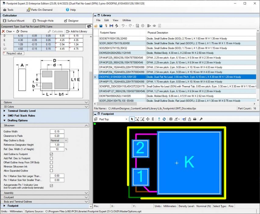 PQFN: 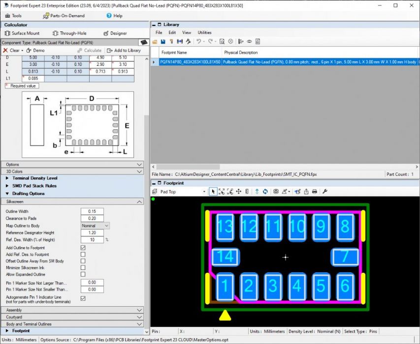 SON:  PSON:  Thanks.
|
Replies:
Posted By: zentekfr
Date Posted: 06 Jun 2023 at 6:20am
|
Notice that things are handled correctly for the Small Outline family (SOIC and SOP), even for very tiny packages. SOP8P50: 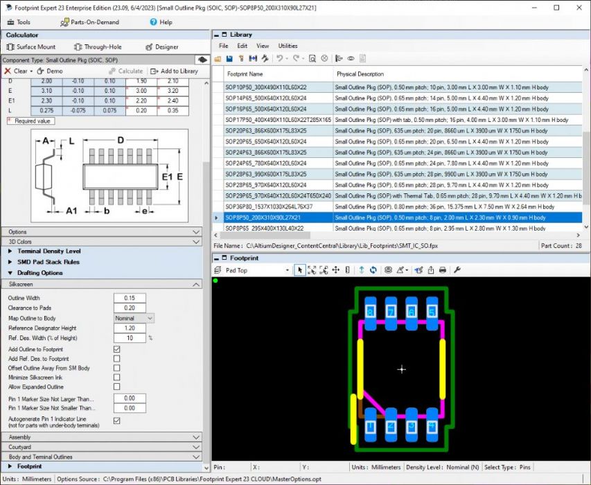 SOP17P50: 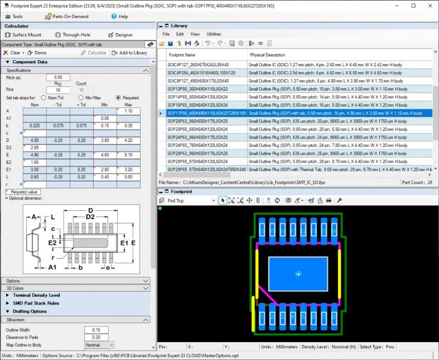 |
Posted By: Tom H
Date Posted: 06 Jun 2023 at 7:39am
|
This was fixed in V23.09 pre-release available here - http://www.pcblibraries.com/downloads" rel="nofollow - www.pcblibraries.com/downloads ------------- Stay connected - follow us! https://twitter.com/PCBLibraries" rel="nofollow - X - http://www.linkedin.com/company/pcb-libraries-inc-/" rel="nofollow - LinkedIn |
Posted By: zentekfr
Date Posted: 06 Jun 2023 at 8:05am
|
Tom, Look at my captures: they are taken from 23.09 dated 6/4/2023. Please note that this is a different concern than the previous one we talked about regarding the Designer. Justin
|
Posted By: Jeff.M
Date Posted: 06 Jun 2023 at 10:03am
|
Assuming that the colors are: brown for body; magenta for assembly otl.; yellow for silkscreen otl.; green for courtyard; blue for pads. The rules for "Allow Expanded (Silkscreen) Outline" and "Offset away from Body" only apply to the relationship between the outline and the body when that spacing is greater than the spacing to a pad. In all of these cases (expanded, offset, or clearance-to-pad) the outline will not represent an accurate geometry. This is apparent in your DFN, PQFN and SON examples. Maybe you're expecting the silkscreen to contour to the body where it can? That can be done in most cases in calculated parts where the finished outline is predictable, but in some (like parts where the pads may be either totally or partially under the body) the variations are too numerous, and it must be simplified to simple lines or rectangles. Outlines are handled differently in FP Designer parts where there is an algorithm that actually can contour the silkscreen. This is required since the outline for any given FPD part may encounter any number of "obstacles" that might interfere with the outline. To allow us to answer specific questions in the future would you please include a reference part, either with dimensions, a data sheet, an fpx file or the 'Demo' part, so we can reproduce an example of your issue and follow along with your inquiry. ------------- Stay connected - follow us! https://twitter.com/PCBLibraries" rel="nofollow - X - http://www.linkedin.com/company/pcb-libraries-inc-/" rel="nofollow - LinkedIn |
Posted By: zentekfr
Date Posted: 06 Jun 2023 at 12:35pm
Jeff,
Understood, thanks.
Not sure to understand what you mean. In which case? What is the "accurate geometry"?
If you mean "map the silkscreen to the body", then yes. Exactly like the calculator would do for a SOIC. Here is an FPX file containing the 4 footprints with "inconsistent" silkscreen outlines: uploads/16707/Silkscreen-outline.fpx" rel="nofollow - uploads/16707/Silkscreen-outline.fpx And here is an extract from the SO family, which, to me, is the example to follow even for bottom lead components: uploads/16707/SMT_IC_SO.fpx" rel="nofollow - uploads/16707/SMT_IC_SO.fpx Justin
|

Posted By: Jeff.M
Date Posted: 07 Jun 2023 at 3:15pm
|
Q. What is the "accurate geometry"? In the confines of this discussion, geometry refers to the graphic representation of the silkscreen outline as created by the FPE software, and its physical relationship to the object component body. An accurate geometry is one that faithfully conforms to the defined object shape that it's meant to represent. A true, accurate geometry would be one that mirrors the true shape of the object. Beyond that are alternate geometries that diverge in varying degrees. The first variation effecting silkscreen geometry is the body material condition - min, max or nominal - which is selected to be the true reference object. Beyond that are options allowing modifications that can be either optional or required: 1.) a shift of the outline in ways to avoid obscuration in the design.; 2.) option to expand or delete segments in order to avoid conflicts that would result in manufacturing or fabrication rule violations.; 3.) option to create an entirely different geometry that constructs a satisfactory shape by avoiding all aforementioned conflicts.; 4.) the possibility that there are no acceptable provisions that will allow for a geometry to be created. The forgoing possibilities can be applied to different extents within the various component families. ------------- Stay connected - follow us! https://twitter.com/PCBLibraries" rel="nofollow - X - http://www.linkedin.com/company/pcb-libraries-inc-/" rel="nofollow - LinkedIn |
Posted By: zentekfr
Date Posted: 09 Jun 2023 at 12:28am
|
Hello Jeff, Thank you for the explanation.
Is this the default behavior for all packages, in that order? Do I have full control over steps 1, 2 and 3 with some software settings? (beyond "Expanded outline" and "Offset outline away") Bridging the gap with my original examples, below is what I would have expected to get in order to be consistent with the rest of my footprints: DFN:  Instead of: SON: 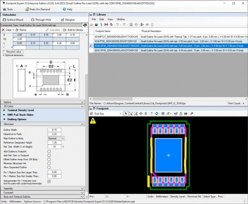 Instead of: Is this something already possible with the latest version of the software?
|
Posted By: Jeff.M
Date Posted: 09 Jun 2023 at 10:22am
|
There are no plans to change any silkscreen outline options except to fix errors that might result in manufacturing or fabrication defects. ------------- Stay connected - follow us! https://twitter.com/PCBLibraries" rel="nofollow - X - http://www.linkedin.com/company/pcb-libraries-inc-/" rel="nofollow - LinkedIn |
Posted By: zentekfr
Date Posted: 09 Jun 2023 at 11:08am
| Understood. |