BGA PAD Mask Definition
Printed From: PCB Libraries Forum
Category: PCB Footprint Expert
Forum Name: Questions & Answers
Forum Description: issues and technical support
URL: https://www.PCBLibraries.com/forum/forum_posts.asp?TID=3271
Printed Date: 26 Jun 2026 at 4:26pm
Topic: BGA PAD Mask Definition
Posted By: mnperry
Subject: BGA PAD Mask Definition
Date Posted: 17 May 2023 at 6:24am
|
I get the idea of either a reduction or increase in defining the land pad based on whether I am defining a collapsing or non-collapsing ball / land pattern. This is a percentage. How is the solder and paste mask (excess) defined? Is there a manual calculation I have to do in the case of an increase in pad size so the mask will partly cover the land pad? In the calculator the solder mask excess is 0.00 no matter whether a collapsiong or non-collapsing ball is being used. 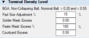 Also in the CAD translator, I see this. What is the UseMaskExpansionRules for? 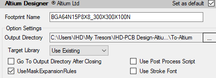 I suspect I am missing something obvious. Thanks.
|
Replies:
Posted By: Tom H
Date Posted: 17 May 2023 at 8:37am
|
Altium has its own Preference Rules and Solder Mask Swell is one of them. UseMaskExpansionRules = no matter what solder mask is defined in Footprint Expert, use the Altium Preference settings. In other CAD tools (like PADS Layout), the solder mask defined in Footprint Expert is translated directly across. Everyone has there own solder mask swell. 0.05, 0.06, 0.07, 0.075, 0.08, 0.09, 0.10, etc. In a typical company PCB Library, every solder mask oversize is the same value. However, an example of changing times, Texas Instruments recommended solder mask swell on fine pitch and microminiature packages is 0.05 swell but in larger pin pitches and bigger packages the mfr. recommended solder mask swell is 0.07. For BGA's TI recommends rounded corner squares for solder mask. There are more and more semiconductors from TI that have complex solder mask shapes.  These semiconductors are becoming more mainstream every day.  ------------- Stay connected - follow us! https://twitter.com/PCBLibraries" rel="nofollow - X - http://www.linkedin.com/company/pcb-libraries-inc-/" rel="nofollow - LinkedIn |