SMPC (TO-277A) made out of DFN standard
Printed From: PCB Libraries Forum
Category: Libraries
Forum Name: Footprints / Land Patterns
Forum Description: [General or a CAD specific issues / discussions]
URL: https://www.PCBLibraries.com/forum/forum_posts.asp?TID=3067
Printed Date: 24 Jun 2026 at 11:08am
Topic: SMPC (TO-277A) made out of DFN standard
Posted By: zentekfr
Subject: SMPC (TO-277A) made out of DFN standard
Date Posted: 23 Feb 2022 at 3:57am
|
Hello, In the process of building a footprint for a SMPC component (standardized against JEDEC TO-277A), I found that a 3-pin DFN could do the job. The obtained land pattern is very close to the manufacturer's recommended footprint. Of course the pins should be reordered/renamed. Is my idea of building this part out of a DFN3 good? Not advisable? And why?   Thanks!
|
Replies:
Posted By: zentekfr
Date Posted: 23 Feb 2022 at 6:06am
|
I add the drawings and datasheet for reference: https://www.vishay.com/docs/89335/ar4pm.pdf 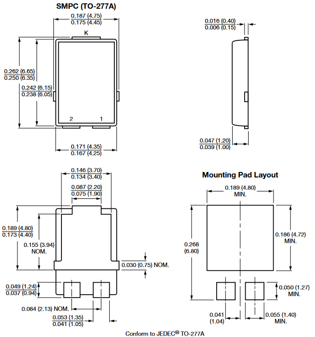
|
Posted By: Tom H
Date Posted: 23 Feb 2022 at 9:45am
|
The Vishay TO-277A Case Code is not a 3-pin DFN component family. This footprint must be created in FP Designer. There are 34 Vishay part numbers on https://www.pcblibraries.com/POD" rel="nofollow - www.pcblibraries.com/POD that have the TO-277A Case Code. Try this one - uploads/3/Vishay_TO-277A.zip" rel="nofollow - uploads/3/Vishay_TO-277A.zip ------------- Stay connected - follow us! https://twitter.com/PCBLibraries" rel="nofollow - X - http://www.linkedin.com/company/pcb-libraries-inc-/" rel="nofollow - LinkedIn |
Posted By: zentekfr
Date Posted: 24 Feb 2022 at 12:58am
|
Hello Tom, Of course it's not a DFN. But as soon as I use the FP Designer, I'm losing much of the features of Footprint Expert (3-tier density system, rounded rectangle pads, pad shapes drawing, Master options for batch generation, ...). That's why I considered building it from a known standard package. Thanks for your answer  Justin
|
Posted By: Tom H
Date Posted: 24 Feb 2022 at 10:42am
|
In FP Designer you have 100% control of the pad stacks like Rounded Rectangle Pads and Pad Shapes. All non-standard package footprints should be created in FP Designer. This is not a 3-Tier Density footprint. Only the mfr. recommended pattern will work correctly. If you need FP Designer training, we can do a quick webcast so I can show you some great features. ------------- Stay connected - follow us! https://twitter.com/PCBLibraries" rel="nofollow - X - http://www.linkedin.com/company/pcb-libraries-inc-/" rel="nofollow - LinkedIn |
Posted By: zentekfr
Date Posted: 25 Feb 2022 at 10:22am
|
So I probably missed the rounded rectangle option. Then a webcast is welcome! I will send you an e-mail.
|