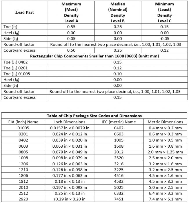
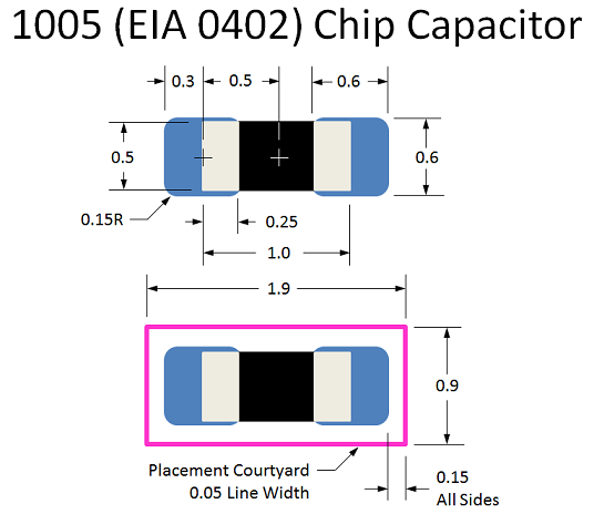
0402 Min Size Land Pattern
Printed From: PCB Libraries Forum
Category: Libraries
Forum Name: Footprints / Land Patterns
Forum Description: [General or a CAD specific issues / discussions]
URL: https://www.PCBLibraries.com/forum/forum_posts.asp?TID=30
Printed Date: 26 Jun 2026 at 5:02am
Topic: 0402 Min Size Land Pattern
Posted By: wolfeman
Subject: 0402 Min Size Land Pattern
Date Posted: 19 Mar 2012 at 11:58am
|
I have a design with 1mm & .8mm pitch BGAs on it. Using 0402 caps on back. Question, does anyone have any input with problems etc using 0402 patterns created using the smallest pattern calculated with current calculator? If I use smallest pattern 0402 it calculates out to about .56mm sq pads on .84mm centers. The 1mm BGA works reasonably well with this size 0402 and with gaps in balls on the .8mm part that smallest pattern could work well too. Any feedback will help. We really can’t switch to 0201s on this project at this time. Thanks Bob |
Replies:
Posted By: Tom H
Date Posted: 19 Mar 2012 at 1:28pm
|
Bob, You’re on
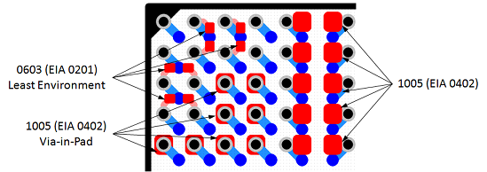
the right track. Use the “Least” environment for EIA 0402 (1005 metric) chip
components. No one should ever use the Most environment for this chip size
due to excessive solder. If you
normally use the “Most” environment for library construction, use the “Nominal”
environment for the 0402 (1005) land pattern. If you
normally use the “Nominal” environment for library construction, use the
“Least” environment for the 0402 (1005) land pattern. Too much solder on this micro-miniature 2-pin component causes tombstoning in the assembly reflow oven (especially when using lead-free solder).
------------- Stay connected - follow us! https://twitter.com/PCBLibraries" rel="nofollow - X - http://www.linkedin.com/company/pcb-libraries-inc-/" rel="nofollow - LinkedIn |
Posted By: mypal_suresh
Date Posted: 09 Oct 2014 at 8:26am
|
Hello Tom, 1.In what all packages we should provide "Terminal " Dimesions as nominal instead of min and max. (ex:0201,0402,0603,0805 packages) 2.Can you be more specific to what is unrealistic tolerances ? In the above attached datasheet link the terminal dimesion is 0.3 +/- 0.1 mm. What would be T min and T max ? http://www.mouser.com/ds/2/40/cx7r-218113.pdf" rel="nofollow - http://www.mouser.com/ds/2/40/cx7r-218113.pdf In this datasheet the terminal size 0.25 +/- 0.15 mm . What would be T min and T max ? Thanks in Advance
Regards
Sureshbabu |
Posted By: Tom H
Date Posted: 09 Oct 2014 at 9:19am
|
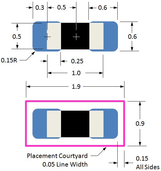
We had a meeting with IPC-7351 committee last week and we adjusted the "TOE" solder joint goal for parts less than 1.6 mm length. So I have to delete the comment about using only Nominal dimensions for the component terminal because we fixed that in the IPC Calculator in the V2014.11 release. Here is the new solder joint goal chart for chip components. These new values for miniature parts will eliminate tombstoning issues and provide the best paste volume for the assembly process.
------------- Stay connected - follow us! https://twitter.com/PCBLibraries" rel="nofollow - X - http://www.linkedin.com/company/pcb-libraries-inc-/" rel="nofollow - LinkedIn |
Posted By: Tom H
Date Posted: 09 Oct 2014 at 9:21am
|
I highly recommend that you download this new paper on Surface Mount Components - http://www.pcblibraries.com/forum/surface-mount-component-families_topic1391.html" rel="nofollow - http://www.pcblibraries.com/forum/surface-mount-component-families_topic1391.html This paper provides the latest component families and terminal types and their related solder joint goal tables. ------------- Stay connected - follow us! https://twitter.com/PCBLibraries" rel="nofollow - X - http://www.linkedin.com/company/pcb-libraries-inc-/" rel="nofollow - LinkedIn |
Posted By: Fynjy
Date Posted: 06 Feb 2015 at 12:21am
|
Hello Tom. How will change the designation CAPC1608X90 if I use the density of A, B, C? |
Posted By: Tom H
Date Posted: 06 Feb 2015 at 7:24am
|
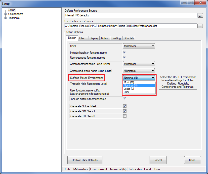
The 1608 is the smallest chip that has 3-Tier Environment Density Levels Least, Nominal and Most). It depends on which version of Library Expert you are using (Pro or Lite) as to where you change the Environment. If you are using Library Expert Lite you change the Environment in the "Terminal > Environment" tab. If you are using Library Expert Pro you change the Environment in "Setup Preferences > User Preferences > Design > Surface Mount Environment > Drop Down" -
------------- Stay connected - follow us! https://twitter.com/PCBLibraries" rel="nofollow - X - http://www.linkedin.com/company/pcb-libraries-inc-/" rel="nofollow - LinkedIn |
Posted By: SandroLanot
Date Posted: 11 Feb 2015 at 2:55pm
|
Hi, This is my 1st post after joining few days ago. Is there any assembly attachment issues if my 0402 land pattern is 0.40 mm x 0.50 mm, with 1.00 mm pitch?
|
Posted By: Tom H
Date Posted: 11 Feb 2015 at 3:06pm
|
Your pad size is the Least Environment. This is good for Nominal.
------------- Stay connected - follow us! https://twitter.com/PCBLibraries" rel="nofollow - X - http://www.linkedin.com/company/pcb-libraries-inc-/" rel="nofollow - LinkedIn |
Posted By: jayx
Date Posted: 29 Mar 2015 at 2:19pm
|
Hello, I was trying to find recommended land pattern design for the most popular packages like 0603, 0805, SO8 etc. but it turns out to be pretty difficult. I found IPC-7351 and its 3-Tier approach but don’t really understand how can I calculate correct pad sizes using these values. Also I've seen PCB Library Expert SMD Reference Calculator but it returns incorrect values - try to enter 1608 (EIA 0603) package dimensions L=1.6, T=0.35, W=0.3 with ±0.15mm tolerance as found in Kemet datasheet http://www.kemet.com/Lists/ProductCatalog/Attachments/351/KEM_CC103_AUTO_SMD.pdf and calculated pads will overlap. Finally I've found information that ModelSource libraries available to download for DesignSpark are created to the IPC-7351 standard. However supposedly also based on IPC-7351 Kemet land pattern design recommendations in document mentioned above (page 12) is slightly different than these in ModelSource. By the way Kemet recommendations are also slightly different for 1005 (EIA 0402) than these in this topic. I know the differences are not big and in real life probably doesn’t matter but would be nice to keep land patterns the same across the industry. So I'm really surprised there are no exact dimensions specified e.g. in IPC-7351 for the most popular packages. |
Posted By: Tom H
Date Posted: 29 Mar 2015 at 2:32pm
|
The Free Library Expert Lite provides all the Land Pattern dimensional data for 144 different component families - http://www.pcblibraries.com/downloads" rel="nofollow - www.pcblibraries.com/downloads You can also switch between IPC-7351 Density Levels. Since the V2015.09 Library Expert Lite has all the latest IPC-7351C mathematical formulas for packages less than 0603, you'll be able to see distinct differences between 0603, 0402 and 0201 chip components. It also has all the rules for Molded Body Tantalum Capacitors and Diodes. The Free Library Expert Viewer can load FPX files and if you purchase the IPC-7351B you get a special Viewer that comes with 5,000 different component package dimensions. http://landpatterns.ipc.org/default.asp" rel="nofollow - http://landpatterns.ipc.org/default.asp ------------- Stay connected - follow us! https://twitter.com/PCBLibraries" rel="nofollow - X - http://www.linkedin.com/company/pcb-libraries-inc-/" rel="nofollow - LinkedIn |
Posted By: jayx
Date Posted: 20 Apr 2015 at 3:54pm
|
Hi Tom, OK, as advised I've downloaded Library Expert Lite and entered 1005 (EIA 0402) dimensions (based on Kemet: D=1±0.05, E=0.5±0.05, A=0.5±0.05. L/L1=0.3±0.1mm) and land pattern results are: L/L1=0.59, W=0.6, S=0.22mm. Very similar to your recommendations apart from S which is two times smaller (it's 0.5mm in your recommendation). It's quite big difference for such a small component, and in fact Kemet recommends S=0.28mm so close to the above calculations. Reducing tolerance or change density level don't get me close to your recommended S dimension, could you comment please? |
Posted By: Tom H
Date Posted: 21 Apr 2015 at 5:48am
|
I don't think you understand Library Expert. The initial settings are IPC-7351 compliant but the user has several options. 1. You can select the Footprint tab and enter the mfr. recommended pattern dimensions. 2. You can open the "Terminal Settings > Density Level" and change the Toe, Heel and Side solder joint goals. 3. Or, what some users are starting to do is in the Terminal tab is change the Placement and Fabrication Tolerances to 0 (zero) due to the accuracy of the machines and processes in 2015. I would not take the IPC-7351 default settings as the holy gospel as the "Standard" was recently downgraded to a "Guideline". And new updated solder joint goals are currently in testing. So maybe the mfr. recommendation is the way to go. Then you can blame any problems on the mfr. ------------- Stay connected - follow us! https://twitter.com/PCBLibraries" rel="nofollow - X - http://www.linkedin.com/company/pcb-libraries-inc-/" rel="nofollow - LinkedIn |
Posted By: DenisFr
Date Posted: 08 Nov 2016 at 3:58am
|
Hi Tom, I try to understand how the footprints are calculated with Library expert. Especialy "S". In IPC, i saw that Sm=Lm-2xTM, but i don't find the same result than in the calculation tab. For example, for a 0805 resistor, i will have Sm=1.85+2x0.65=0.55 while i obtain 0.816 in library expert. Did i miss a parameter ? Thank you very much Denis
|
Posted By: Tom H
Date Posted: 08 Nov 2016 at 7:49am
|
You should download the Surface Mount Reference Calculator and it will allow you to change all the values so you can see how the IPC mathematical model works. http://www.pcblibraries.com/downloads" rel="nofollow - www.pcblibraries.com/downloads If you're using V2016.14 it's in this folder - C:\Program Files (x86)\PCB Libraries\Library Expert 2016\Documents The IPC math considers the Component Package and Terminal Lead Tolerance and adds a Fabrication and Assembly Tolerance plus a Toe, Heel and Side solder joint goal. ------------- Stay connected - follow us! https://twitter.com/PCBLibraries" rel="nofollow - X - http://www.linkedin.com/company/pcb-libraries-inc-/" rel="nofollow - LinkedIn |
Posted By: DenisFr
Date Posted: 09 Nov 2016 at 1:20am
| Great, thank you very much. I see the formula used so it can be more precised i believe. |