No Option For Pad Round-off In V2021 Edition?
Printed From: PCB Libraries Forum
Category: PCB Footprint Expert
Forum Name: Questions & Answers
Forum Description: issues and technical support
URL: https://www.PCBLibraries.com/forum/forum_posts.asp?TID=2866
Printed Date: 26 Jun 2026 at 1:44pm
Topic: No Option For Pad Round-off In V2021 Edition?
Posted By: ExplodingWaffle
Subject: No Option For Pad Round-off In V2021 Edition?
Date Posted: 07 Apr 2021 at 4:29am
|
Hello- just upgraded to the new version of the software. Enjoying custom footprints and FPX libraries in the free version! Sort of bummed about 3D STEP being gone- while it certainly made my 3D views look a lot nicer in Kicad, I suppose they aren't needed. One thing that I do need that seems to have gone missing from the new version is courtyard and pad-roundoff - is it just gone, or am I missing it? I layout my boards on a grid so it's a very useful feature for me. |
Replies:
Posted By: Tom H
Date Posted: 07 Apr 2021 at 8:01am
The new V2021 Footprint Expert for KiCad now has these new features:
Options have min/max decimal place accuracy up to 6 places. Library Editor saves your package dimensions, personal polarity markings, custom 3D STEP color, footprint rotation and footprint pad stack dimensions. Select the Footprint panel and enter your pad length x width x gap and save to FPX. You have 100% control now of every pad size and snap grid. The 3D STEP is no longer free. You need to pay the yearly maintenance of $299 so we can generate the revenue to enhance that feature with top programmers. You need to move up to the Enterprise version of Footprint Expert for $99 for KiCad. There are no banner ads in the Enterprise version. Let us know if you need any help in understanding all the new features in V2021. Create your personal FPX file. Create your personal Option file. ------------- Stay connected - follow us! https://twitter.com/PCBLibraries" rel="nofollow - X - http://www.linkedin.com/company/pcb-libraries-inc-/" rel="nofollow - LinkedIn |
Posted By: SWB01
Date Posted: 07 Apr 2021 at 8:18am
|
I don't see the roundoff options in 2021 either. Previous versions had roundoff options all over the place, for just about every footprint element, and I used them extensively to snap geometry to my grid as much as possible.
|
Posted By: Jeff.M
Date Posted: 07 Apr 2021 at 9:46am
|
"Roundoff" options are now global and located in 'Tools > Options > Console > Design' in the group 'Decimal Place Accuracy'. 'Minimum' is the minimum number of decimal places to apply. For example a value of 4.1 with a minimum DP value of 2 will round and display as 4.10. 'Maximum' is the maximum number of decimal places to apply. For example a value of 4.123456 with a maximum DP value of 4 will round and display as 4.1234. Different numeric units (mils, millimeters, etc.) have their own settings. Grid placement has it's own setting in the footprint window under the icon 'Manage Layer Display' as Space X and Space Y, emanating from the origin. ------------- Stay connected - follow us! https://twitter.com/PCBLibraries" rel="nofollow - X - http://www.linkedin.com/company/pcb-libraries-inc-/" rel="nofollow - LinkedIn |
Posted By: SWB01
Date Posted: 07 Apr 2021 at 2:25pm
That's not the same thing. I work on an 0.05-mm grid in Altium. To the extent possible/reasonable (subject mainly to the pin pitch), I want all geometry aligned to this grid. In previous versions, I could accomplish this with roundoff values of 0.05 and 0.10 mm, depending on the parameter. In this version, we can only round to a certain number of digits, and the smallest number of digits we can round to (in millimeters) is 2. This is equivalent to a roundoff value of 0.01 mm. There is no longer any way to specify a roundoff value of 0.05 mm or 0.10 mm. That's disappointing. I was hoping for increased flexibility and control over roundoff in this version, not less. In a perfect world, the software would initially do all the calculations at full precision and then stretch and contort it according to some heuristics and intelligence to snap all edges, pad centers, and vertices to my preferred roundoff grid. I'm going to have to keep using the older version until at least the old roundoff behavior is restored. (I was so distracted by the lacking/poor hi-resolution monitor support during the beta that I never noticed that core functionality had been changed or removed. Now I'm wondering if there's anything else important that I've missed.)
We don't mean the grid within Footprint Expert. We mean making footprints compatible with the layout grid we use in our PCB software.
|
 Jeff.M wrote:
Posted By: ExplodingWaffle
Date Posted: 08 Apr 2021 at 2:55am
What SWB said :) roundoff is a nice feature to have routing on a grid. In addition, decimal place is global- just today I had to go to 4 decimal places to make a complicated IC in the FP designer, but I don't think I'd like to use the same settings on say a 1206 or larger part.
Also- today I discovered that setting "Cathode/Anode Pin Names" to Numeric just doesn't do anything, which is 100% a bug. |
Posted By: Ian S
Date Posted: 08 Apr 2021 at 4:08am
|
I agree with SWB01, the new FPX version is unusable without restoring roundoff functionality. For example, in V2020 I had the Terminals>Through Hole>Pad Size Roundoff set to 0.05 mm. This resulted in pad diameter and, more importantly, the through hole (drill) size rounding to 0.05 mm. With the new FPX version the through hole (drill) minimum resolution is 0.01 mm which is not a real world practical resolution when (in my experience) PCB fabricators use drill sizes with 0.05 mm resolution. |
Posted By: Tom H
Date Posted: 08 Apr 2021 at 10:55am
|
We are going to add a new feature in the Pad Stack Rules for PTH hole size roundoff. If your holes are rounded to 0.05 and your pad size calculation multiplier is 2.00 your pad size will always be in 0.05 mm increments. You can now go to 2 decimal place for minimum or 6 places. Same for Maximum. This is vastly superior to any CAD tool in existence. 2 decimal places = 0.01 mm rounding. If you want your SMD pad to be in 0.05 mm increments, open the "Footprint" panel and select "Use Mfr. Recommended Pattern" and enter any value you want. You have the ability to round Up or Down. Here is a sample QFN and the Footprint pad size values that you can round Up or Down to get your desired result. 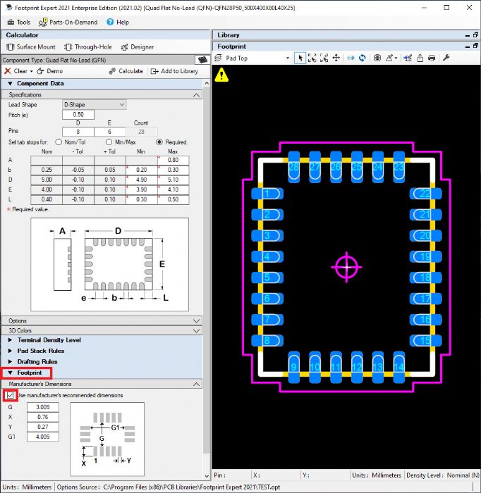 ------------- Stay connected - follow us! https://twitter.com/PCBLibraries" rel="nofollow - X - http://www.linkedin.com/company/pcb-libraries-inc-/" rel="nofollow - LinkedIn |
Posted By: Tom H
Date Posted: 08 Apr 2021 at 11:44am
|
All reported bugs, including the Anode/Cathode numeric pin names are fixed in the V2021.02 release. It only takes us 5 - 10 minutes to fix a bug, so please send me all bug issues directly. ------------- Stay connected - follow us! https://twitter.com/PCBLibraries" rel="nofollow - X - http://www.linkedin.com/company/pcb-libraries-inc-/" rel="nofollow - LinkedIn |
Posted By: Quist
Date Posted: 09 Apr 2021 at 3:33am
|
I don't understand this with rounding of pads. In Options I have set Unis to mm and Minimum and Maximum Decimal Place Accuracy to 2. If I calculate a footprint the dimensions under "Manufacturer's Dimensions" (strange name if this is the calculated dimensions by Footprint Expert) are presented with 3 decimal places. +- 0.005 mm in pad size can't have any practical meaning when it comes to soldering etc so I would like it to stick with 2 decimal places. For larger pads even 1 decimal place would be good enough and dramatically reduce the number of pads in our library. With your solution above Tom, we have to manually edit the dimensions of all pads, this can't be the purpose?
|
Posted By: Tom H
Date Posted: 09 Apr 2021 at 8:36am
|
The Land Pattern Naming Convention must have 3 places because of the way it was designed and created. XX.XX for the values. 2 places to the left of the decimal point and 2 places to the right of the decimal point. I guess you didn't understand 2 X 2 Decimal Place Accuracy like you set in the Console Options. Was this the problem that wasn't really a problem? When you select Decimal Place Accuracy to 2 min and 3 max, it still produces the same footprint name because that is the standard naming convention. i.e.: you can't change the naming convention regardless of your Decimal Place Accuracy because the naming convention is a standard XX.XX for now according to IPC-7351. Note: all leading zero's "0" are dropped and ending zero's are not. ------------- Stay connected - follow us! https://twitter.com/PCBLibraries" rel="nofollow - X - http://www.linkedin.com/company/pcb-libraries-inc-/" rel="nofollow - LinkedIn |
Posted By: Quist
Date Posted: 09 Apr 2021 at 11:07am
|
Ah, no I was not referring to the Naming Convention but rather to the actual pad dimensions presented under Footprint -> Manufacturer's Dimensions. I got the impression that no matter what decimal accuracy I put in I got three decimal places on the dimensions but now I can't reproduce the behaviour so it was probably user induced... I see in our fpx library that we have a different number of decimal places on the pads for different components. That might have been whats fooled me. Can you please comment on the subtitle "Manufacturer's Dimensions". Who is Manufacturer referring to, component manufacturer or PCB manufacturer? I find it a bit confusing. Wouldn't it be better to call it something like "Pad dimensions" and the checkbox something like "Use custom dimensions" or similar? |
Posted By: Tom H
Date Posted: 09 Apr 2021 at 11:42am
|
The Manufacturer reference is the Component Manufacturer, not the fabrication or assembly shops. The current pad stack and footprint naming conventions are intentionally created in 0.01 mm increments because if you added one more place to accommodate 0.001 accuracy, the footprint name would be too long for most CAD tools. Right now, the character limit for a footprint name is 40 characters. If you added one more number to each value the footprint name would be 47+ characters. Body Length X Width X Height X Lead Width X Length X Thermal Tab Width X Length Same with Pad Stack names. ------------- Stay connected - follow us! https://twitter.com/PCBLibraries" rel="nofollow - X - http://www.linkedin.com/company/pcb-libraries-inc-/" rel="nofollow - LinkedIn |
Posted By: Quist
Date Posted: 09 Apr 2021 at 12:34pm
|
I agree, 0.01 mm is good for naming no matter what the physical accuracy is. I even seriously doubt that there is any practical benefit with going below 0.01 accuracy. Normal trace tolerance in an etch proces is probably around 0.05 mm and might be tweaked down to 0.02 mm. Regarding "Manufacturer's Dimension": If I open a part in Footprint Expert and would like to see the size of the pads calculated by Footprint Expert the only way I know to do it is to go to the "Manufacturers Dimensions" section and look there. However, this is not the manufacturers dimensions but rather the dimensions calculated by Footprint Expert. I don't think the naming is intuitive. |
Posted By: Tom H
Date Posted: 09 Apr 2021 at 1:20pm
|
The pad stack naming convention used in Footprint Expert is available for free download on www.pcblibraries.com/downloads In Footprint Expert you can double click (or single click + RMB > Properties) any pad and the program will open the pad Properties. 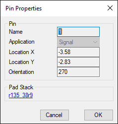 If you select the Pas Stack name, it will open the Pad Stack Manager. 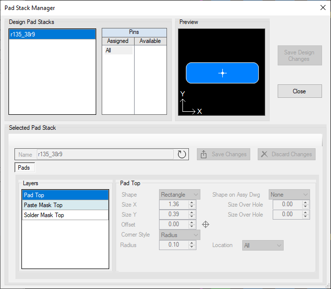 The values are grayed out for any Calculator footprint because if you edit it, PCB Libraries, Inc. or IPC cannot be responsible for any typos. But you can visually see the pad length and width and corner radius too. I can look at any pad stack name and tell you the length, width and corner radius. You can control the corner radius in Options > Pad Stack Rules > SMD Corner Rounding > Corner Size Limit The default is 0.25 but many users change that value to 0.10 or 0.05. ------------- Stay connected - follow us! https://twitter.com/PCBLibraries" rel="nofollow - X - http://www.linkedin.com/company/pcb-libraries-inc-/" rel="nofollow - LinkedIn |
Posted By: arendhagedoorn2
Date Posted: 16 May 2021 at 11:24pm
|
Hi Tom, I've read all the posts about this issue but
there is not realy a solution for the now missing pad round off. Is it
not possible to implement the pad round off just like it was in the
previous versions?: 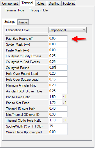 Thank you and best regards, Arend
|
Posted By: Tom H
Date Posted: 17 May 2021 at 12:25pm
|
We're taking a look at adding the Plated Through-hole pad size round-off in V2021.05 this week. The default value will be set to 0.01 but you can change it to whatever value you want. Thanks for the input. ------------- Stay connected - follow us! https://twitter.com/PCBLibraries" rel="nofollow - X - http://www.linkedin.com/company/pcb-libraries-inc-/" rel="nofollow - LinkedIn |
Posted By: Jeromeli
Date Posted: 16 Jun 2021 at 10:42pm
| So is there a solution to this problem? Maybe we need to wait for a higher version? |
Posted By: Tom H
Date Posted: 17 Jun 2021 at 8:18am
|
We added through-hole pad and hole size roundoff feature in V2021.08. Look in Tools > Options > Terminals > Through-hole Change the values to whatever you want. 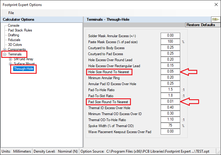 ------------- Stay connected - follow us! https://twitter.com/PCBLibraries" rel="nofollow - X - http://www.linkedin.com/company/pcb-libraries-inc-/" rel="nofollow - LinkedIn |
Posted By: Tom H
Date Posted: 02 Mar 2022 at 11:36am
|
The latest V2022.03 release has a new Options feature for Pad Size Rounding. 2 = 0.01 round-off 3 = 0.001 round-off If you want a 0.05 round-off, select and open the Footprint panel and select "Use mfr. recommended pattern" and change the pad size to whatever you want. This process only takes 30 seconds. Note: IPC has no guidance on SMD pad size rounding. So, when you apply a 0.05 mm SMD pad size round-off, it's not IPC compliant per the 3-Tier Density Levels defined in the IPC-7351 guideline. Using a SMD pad Size Round-off of 0.05 mm cannot be classified as an IPC compliant pattern. The Pad Stack Naming Convention is in 0.01 mm increments. ------------- Stay connected - follow us! https://twitter.com/PCBLibraries" rel="nofollow - X - http://www.linkedin.com/company/pcb-libraries-inc-/" rel="nofollow - LinkedIn |
Posted By: sot23
Date Posted: 26 Jan 2023 at 9:08am
|
I must agree with what is said about the lack of place & size round off. I understand that it is not IPC compliant but it sure was handy to match grid ! Another issue I see with the lack of this functionality : different part manufacturer often describe slightly different tolerances for the same packages. With lands rounded to 0.01mm, we will end up with a lot of different footprints for the same package. One for the (let's say) Infineon Part, one for the On Semi part... For exemple : The demo SOD package in Footprint Expert has a pin width (b dimension) between 0.55mm and 0.75mm. It gives this padstack : r77_87m97_107r19 If I change the pin dimension to 0.56mm-0.74mm (0.01mm difference on both dimensions), the padstack now is : r77_86m97_106r19 I think that this will create a lot of duplicates in our footprint library because unattentive designers will not take the 2 seconds needed to check if the first padstack could acomodate the second pin size (smaller in all it's dimensions). I don't know if I am easily understandable. It is great that we can change it using the "Use mfr. recommended pattern" option though. But I know some designers that will not take the 30 seconds needed to do the change. We sold them an "automatic footprint creation software", they will want it to be fully automated :p Another slight issue I have found with the way values are rounded (using the Decimal Place Accuracy option) is in the naming of the padstacks. If we use the demo QFN (with thermal tab) with a Decimal Place Accuracy of min:2; max:2, the name given to the padstack is r73_30m93_50r7. But the padstack is actually a 0.74mmx0.30mm rectangle (not 0.73mmx0.30mm). 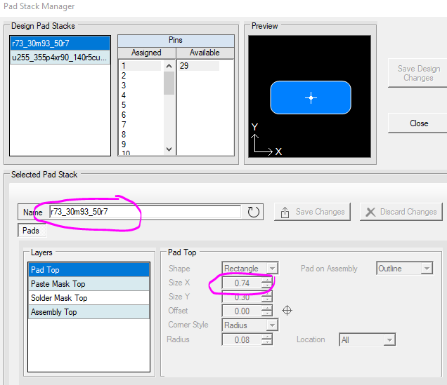 I think this is due to the fact that, when Decimal Place Accuracy is set to min:2, max:3, the actual length of the padstacks is 0.737mm. That gives the r73_30m93_50r7 naming. But that naming isn't updated when using min:2, max:2 accuracy. I rebooted the software but the issue is still there. Anyway, thank you for that great software. It offers tremendous flexibility and the user interface is great in my opinion.
|
Posted By: Tom H
Date Posted: 26 Jan 2023 at 9:17am
|
You can round off the pad stacks any way you want using the "Mfr. Recommended Pattern" panel in the Calculators. Round up or down whatever you want. Also, the "Tools > Options > Console > Pad Size > 2 Places" with round all pad sizes to 0.01 mm increments. If you want 0.05 mm increments us the "Mfr. Recommended Pattern" panel. ------------- Stay connected - follow us! https://twitter.com/PCBLibraries" rel="nofollow - X - http://www.linkedin.com/company/pcb-libraries-inc-/" rel="nofollow - LinkedIn |
Posted By: daniel.lange
Date Posted: 12 Jul 2023 at 1:59am
|
can you explain that more? If you want 0.05 mm increments use the "Mfr. Recommended Pattern" panel. I don't get that. In the end I would like to have a calculation where everything is roundoff to 0.05 mm Pad sizes and Positions. only so I can reuse Pad Stacks and have a small Padstacklib and all my cells follow some grids. In old Library Expert version it was easy to config and now ... I don't know. My entry. Is that the calculation now? if so, I need that in roundoff 0.05 (to do manual it wouldn't be correct) Here I did my best. Is there really no other way to calculate with roundoff 0.05 in the first place, like it did in old version? |
Posted By: Tom H
Date Posted: 12 Jul 2023 at 8:29am
|
Then you should stay with the old version of V2020.03 Library Expert. Footprint Expert follows the IPC-7351 for the mathematical model for pad stack calculation. The IPC-7351 mathematical calculation includes the Fabrication & Assembly Tolerances, the Package and Terminal Lead Tolerances, the Toe, Heel and Side solder joint goals and everything is rounded to the nearest 0.01 mm increment. If you round the pad stack dimensions up or down to 0.05 mm increments for pad size, then it's not IPC-7351 compliant. Also, if you round the pad stack dimension up or down, do you really want to round Down? Or just round everything Up? If you can answer this question then you should be able to open the Mfr. Recommended Footprint panel and manually round all values up to 0.05 increments and you will not get a Density Level suffix of L, N or M in the Footprint Name because it's your pad stack dimensions and not the IPC-7351 calculation. ------------- Stay connected - follow us! https://twitter.com/PCBLibraries" rel="nofollow - X - http://www.linkedin.com/company/pcb-libraries-inc-/" rel="nofollow - LinkedIn |
Posted By: daniel.lange
Date Posted: 13 Jul 2023 at 6:38am
|
You say if you round the calculated values its not compliant to IPC-7351. But the V2020.03 did round it, so that means that the old version isnt IPC-7351 compliant. But you suggest that I should use the old version. Sorry thats not logical for me. Of course its compliant to round up padsizes and round up or down pin positions and gaps between pads. the goal is to have less padstack geometries and nice pin postiongrid for easier fanout and routing. A good librarian and a skilled layouter will like that. All our lib is in 0.05mm steps (only some big CPUs will have 0.001mm accuracy, but for them i dont need that tool) Interesting that I am not the only one who miss that feature for clean library build up. I am disappointed that the feature is gone and that you dont understand why its important. the manual input for manufacturer recommendation will not help with that topic, becasue you can type in every value But yes I will go back to the old version of the tool, thanks for that advice. thats the solution for that. |
Posted By: Tom H
Date Posted: 13 Jul 2023 at 8:10am
|
Many companies are still using V2020.03 Library Expert and will be for years to come. ------------- Stay connected - follow us! https://twitter.com/PCBLibraries" rel="nofollow - X - http://www.linkedin.com/company/pcb-libraries-inc-/" rel="nofollow - LinkedIn |
Posted By: daniel.lange
Date Posted: 19 Jul 2023 at 1:50am
| Would you please provide an official download link? my local distributor cskl only provide the last 2023 version, thanks |
Posted By: Nick B
Date Posted: 19 Jul 2023 at 2:33am
|
I will send you an email. ------------- Stay connected - follow us! https://twitter.com/PCBLibraries" rel="nofollow - X - http://www.linkedin.com/company/pcb-libraries-inc-/" rel="nofollow - LinkedIn |